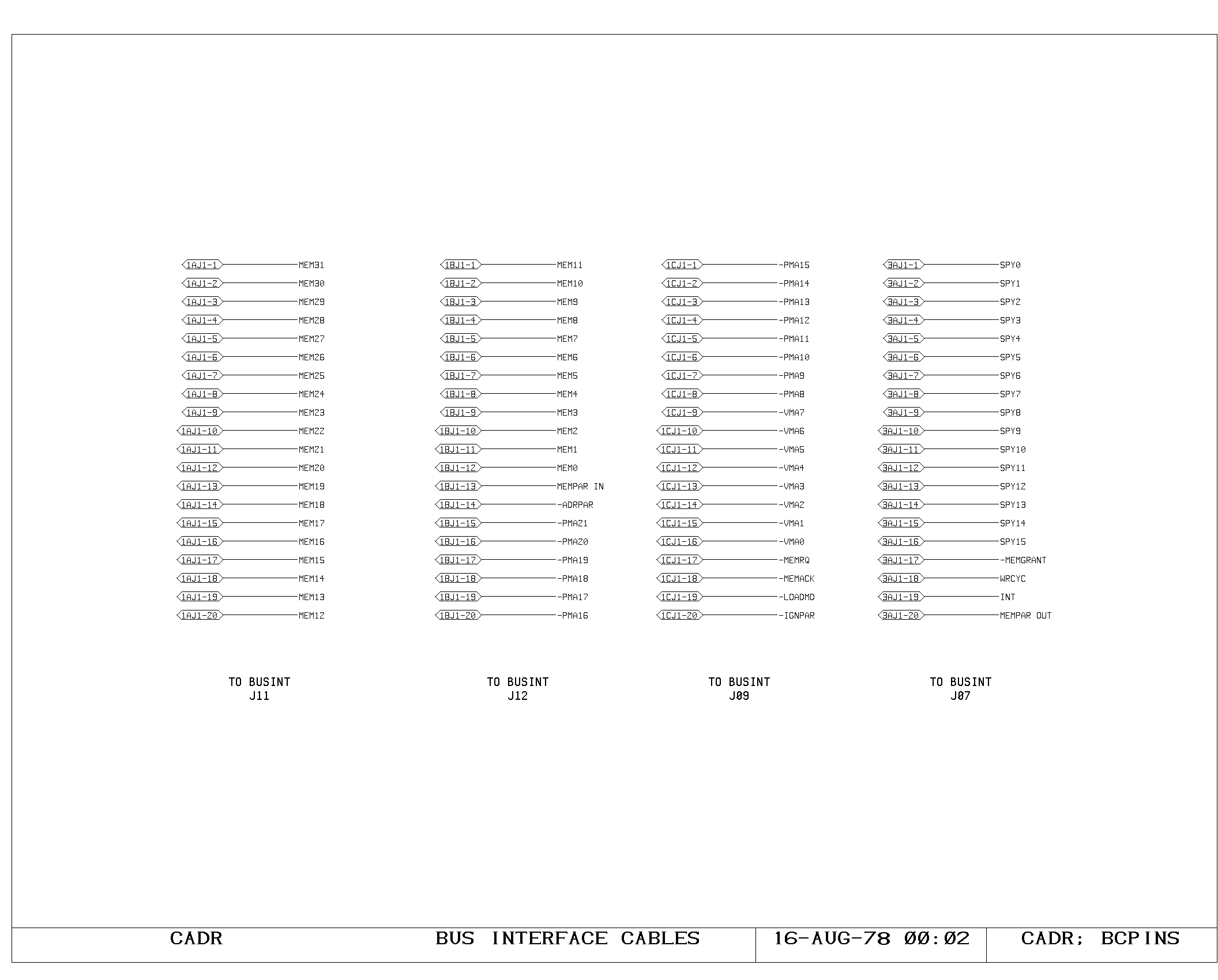
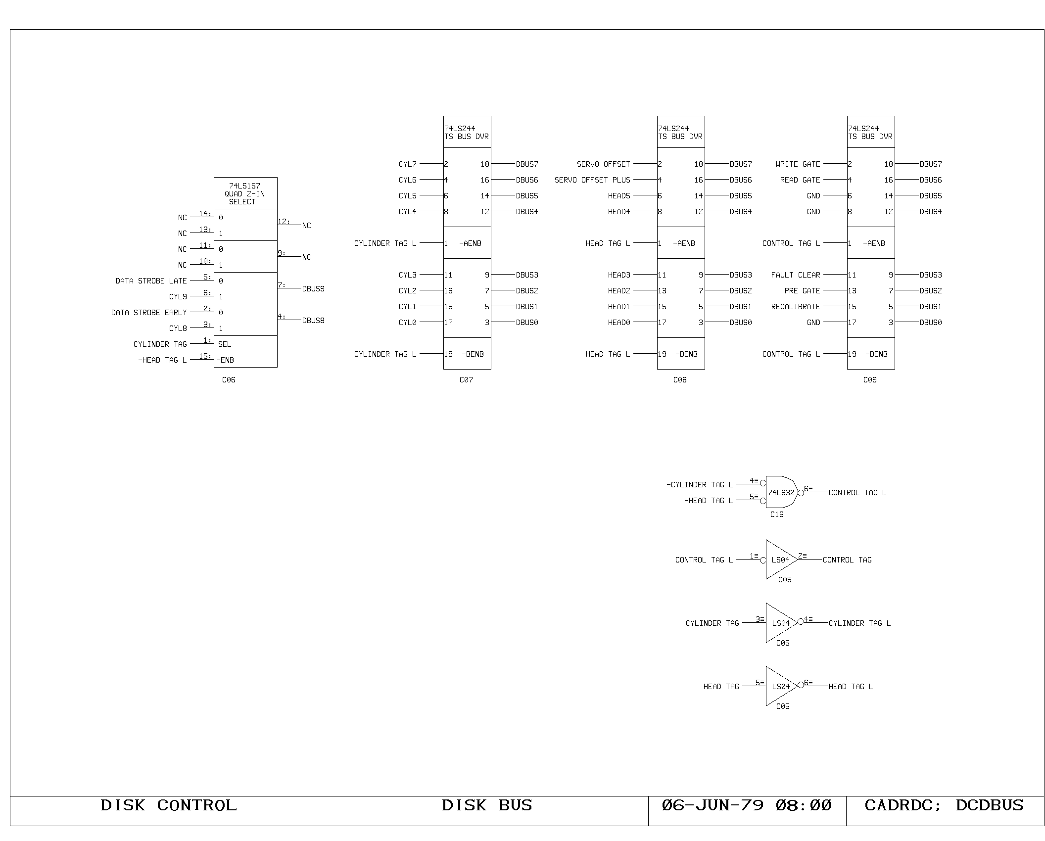
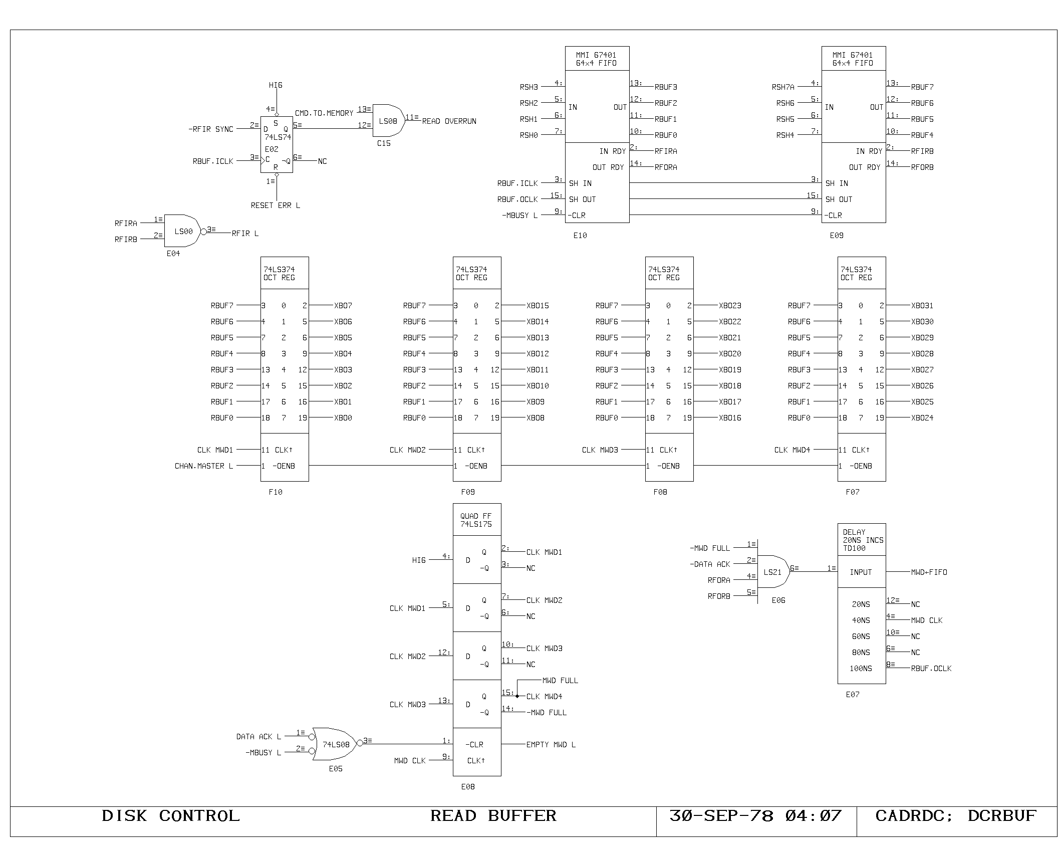
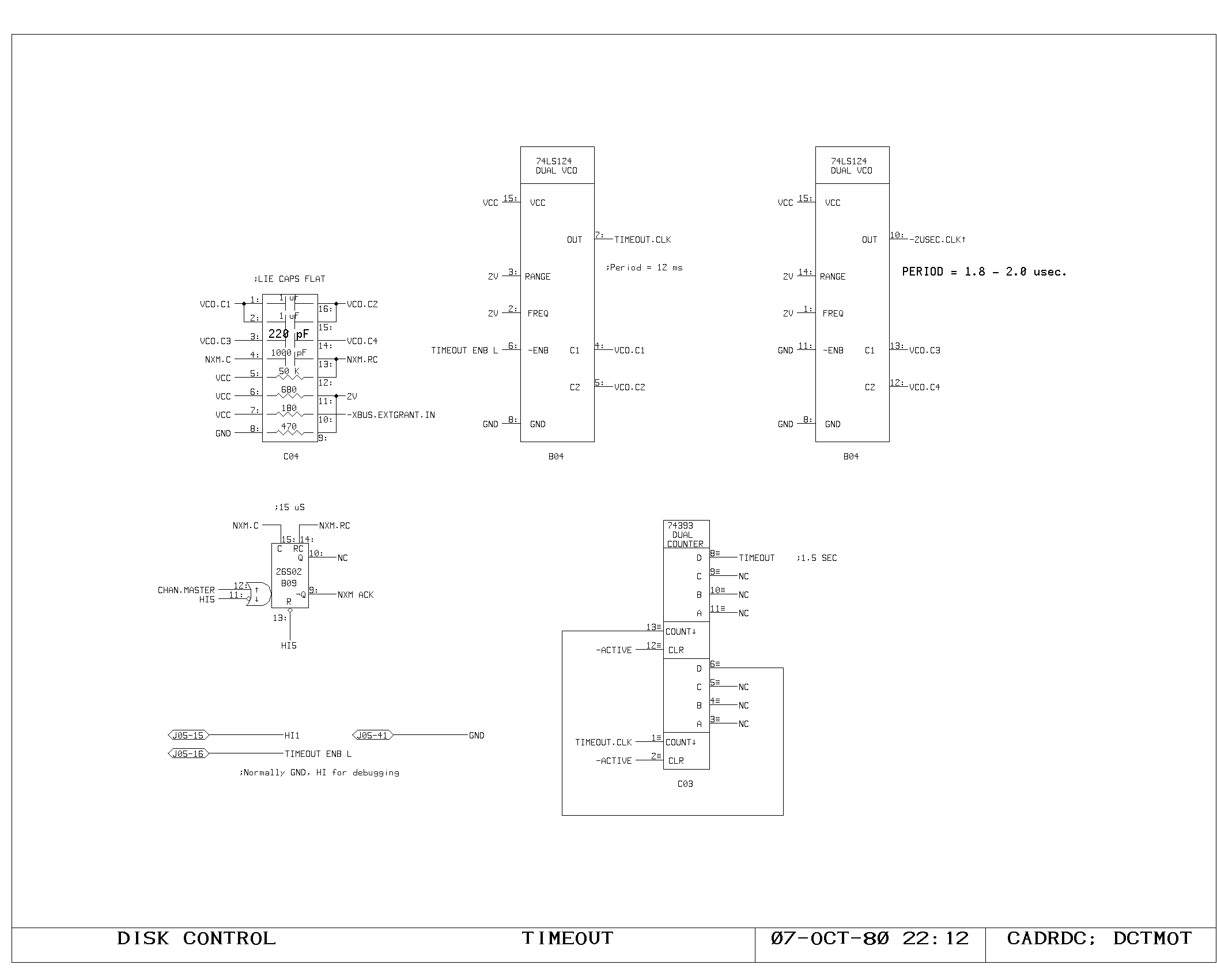
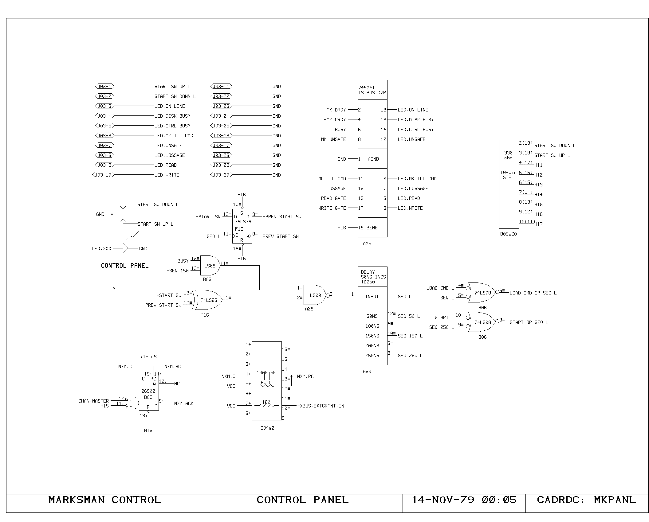
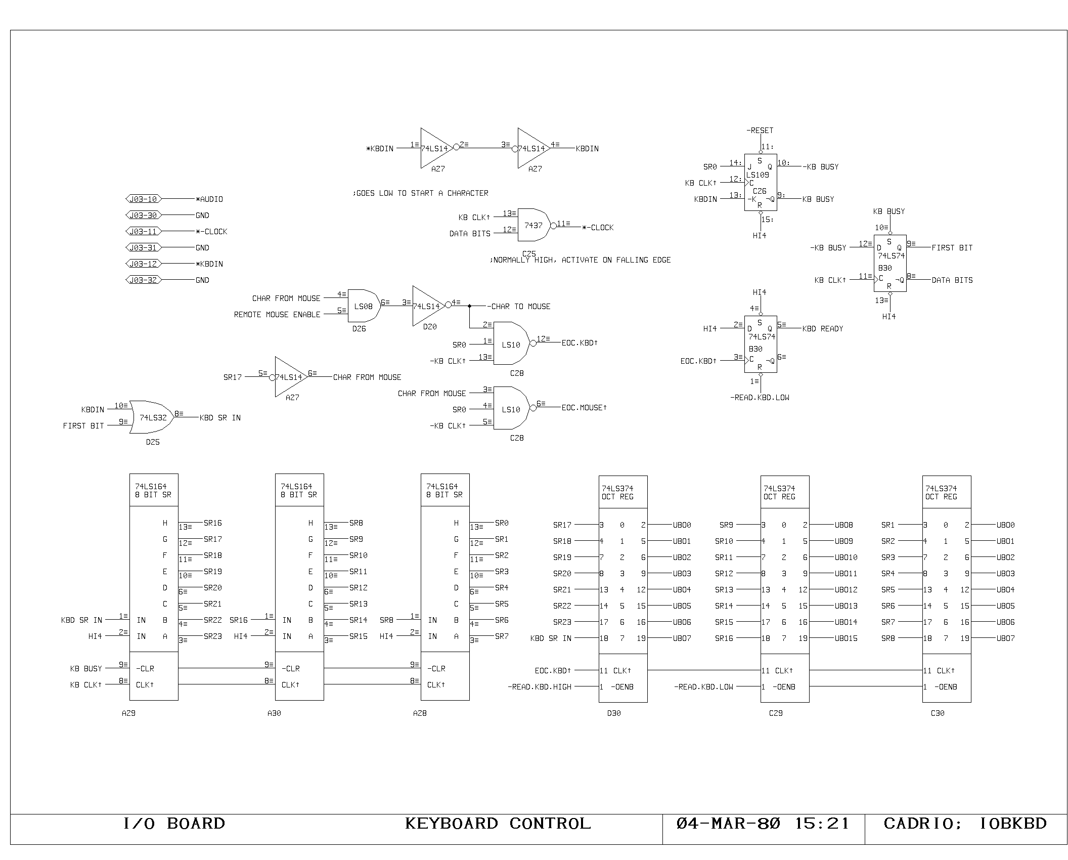
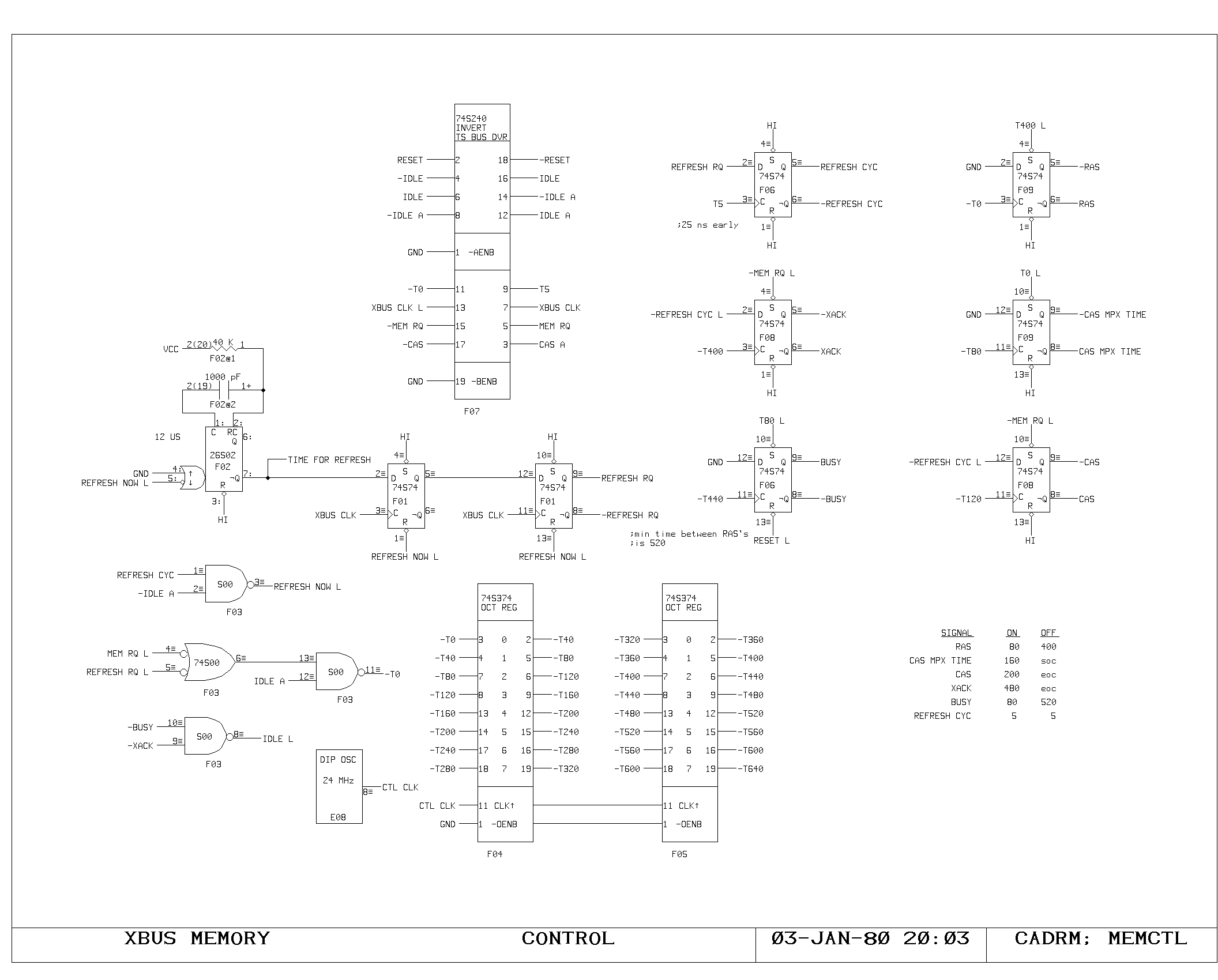
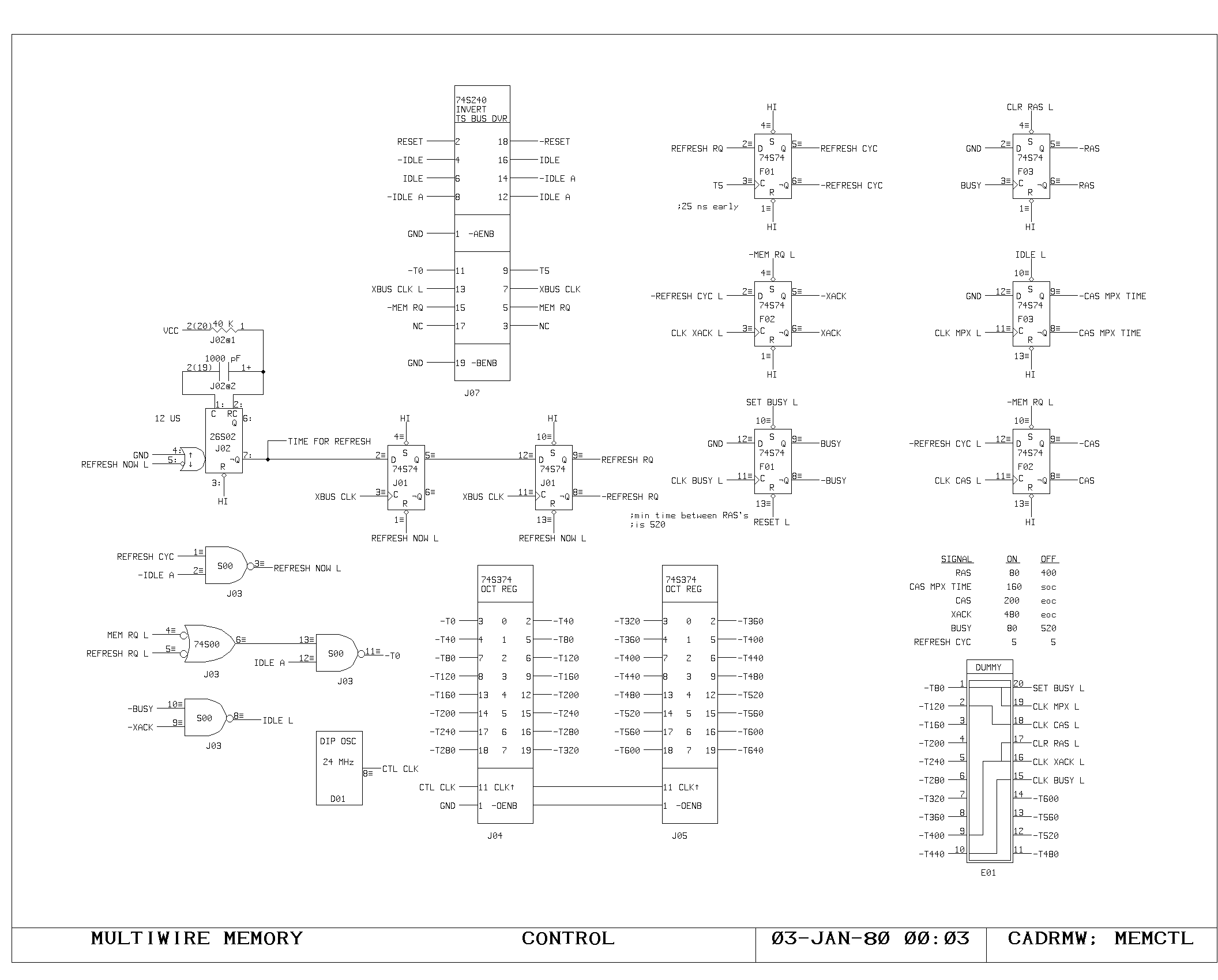
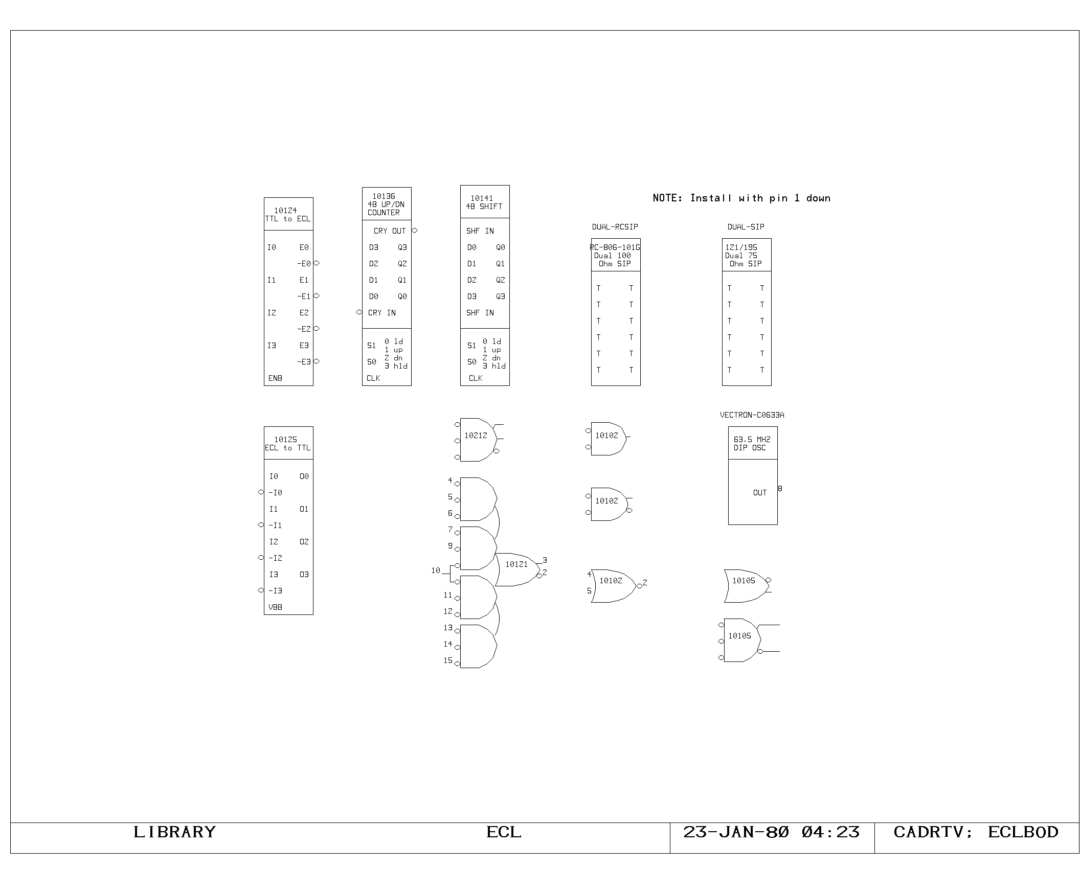
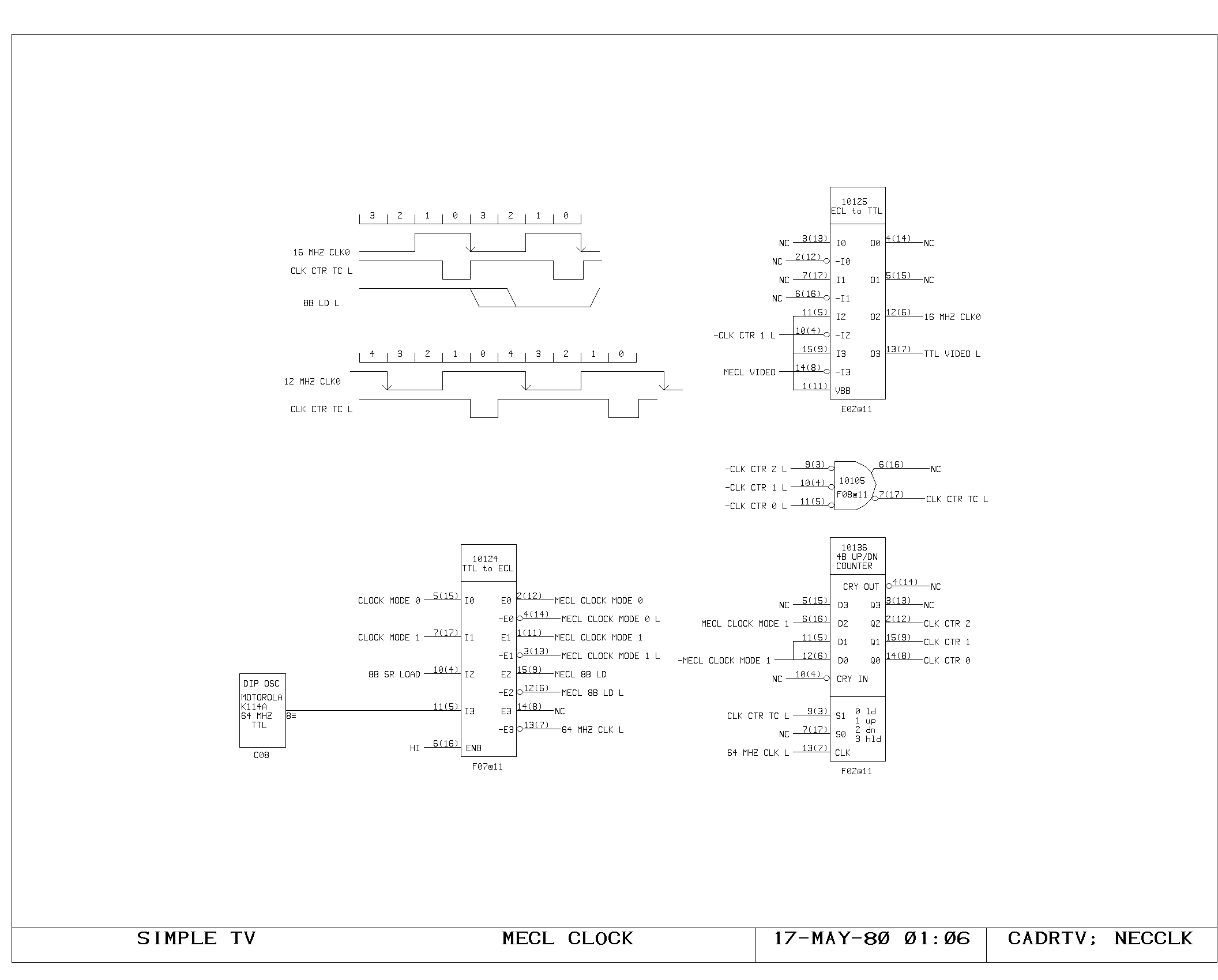
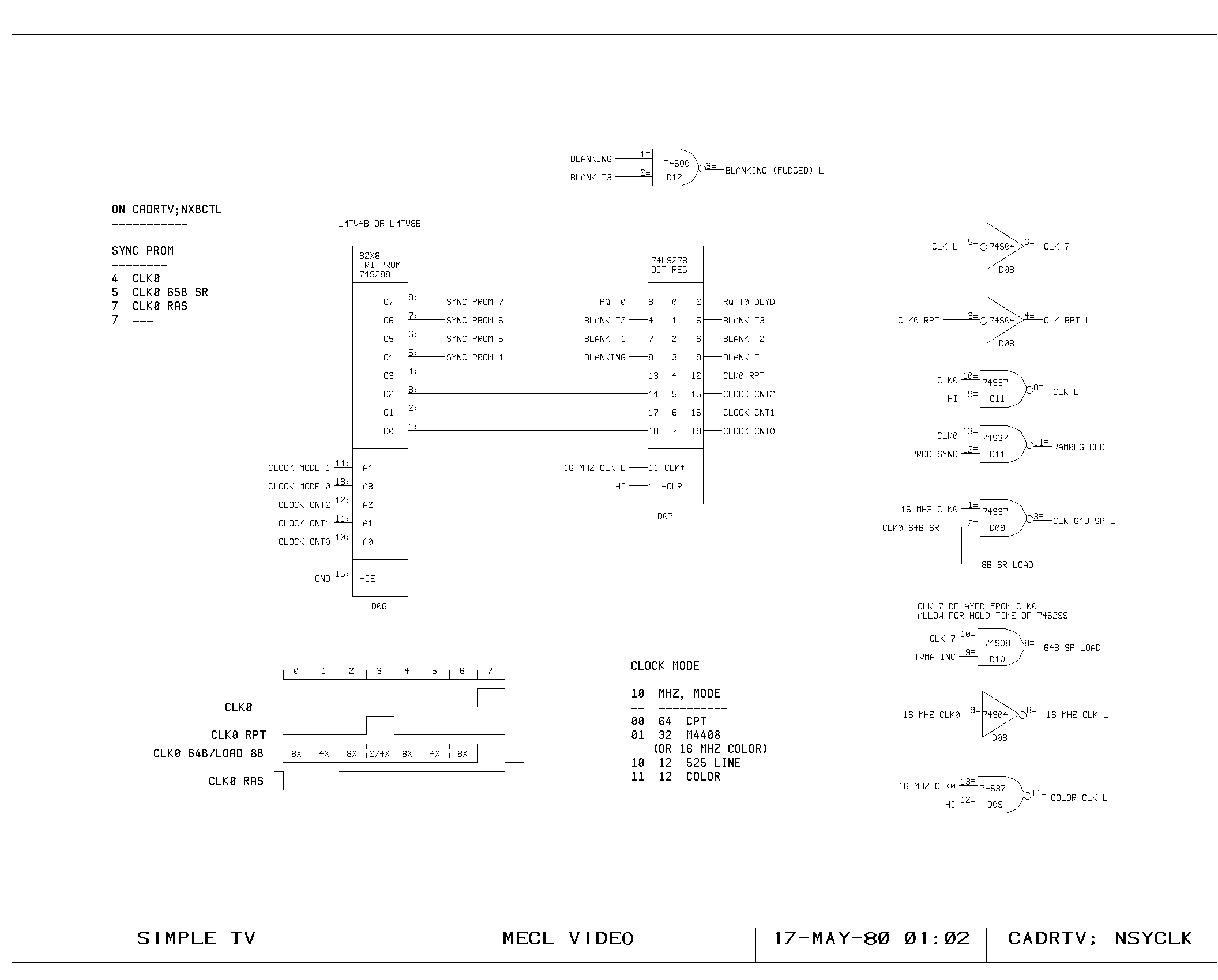
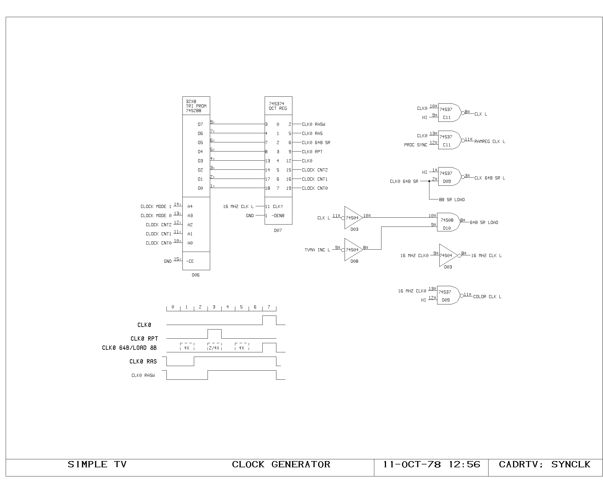
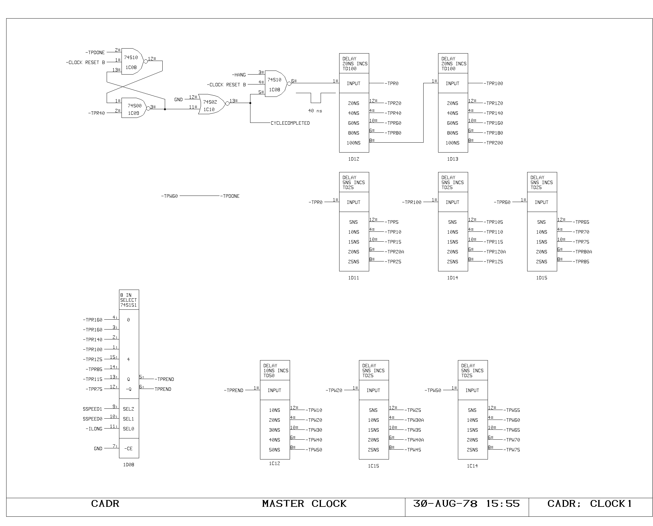
Clock Generation
The main clock for the processor is of approximately 180 nanosecond
period, with roughly equal phases. The processor registers are clocked
on the rising edge of this waveform, which marks the beginning of a
new processor cycle.
Memory devices in the processor requiring write pulses are written by
a write pulse occurring during the second (low) phase of the main
processor clock.
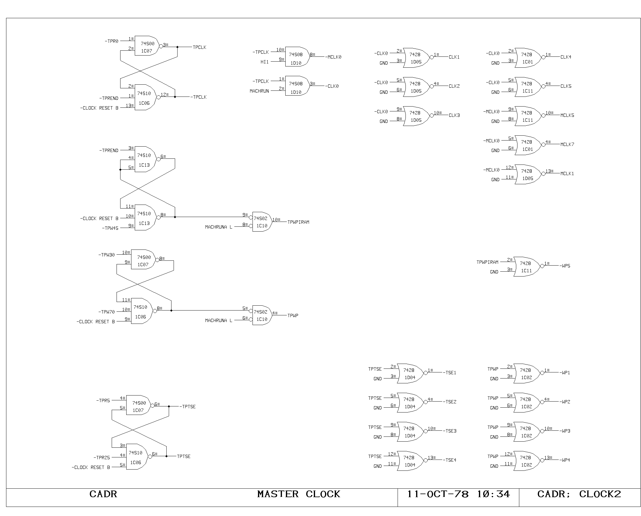
These fundamental timing signals are generated by the circuity on the
CLOCK1 and CLOCK2 prints. Initially, the cross coupled nand flip flop
in the upper left corner of the CLOCK1 print is set, either by
completion of the previous cycle or by power up reset of the
processor. In the absence of the HANG signal indicating a main memory
response delay, the rising edge of the CYCLECOMPLETED flip flop
travels down the series of tapped delay lines, producing the sequence
of TPRxx signals. TPR40 is used to clear CYCLECOMPLETED, establishing
the width of the pulse in the delay lines at about 40 nanoseconds.
The rising edge of the main processor clock is produced by TPR0, which
sets the TPCLK flip flop on the CLOCK2 print. Depending upon the speed
with which the processor is running, a selected pulse from the TPRxx
chain is gated into TPREND, which both clears TPCLK, establishing the
time of fall for the main processor clock, and initiates the TPWxx
delay line pulse. The TPWxx timing chain is used to produce the
processor write pulse, and TPDONE which sets CYCLECOMPLETED in
preparation for a new processor cycle.
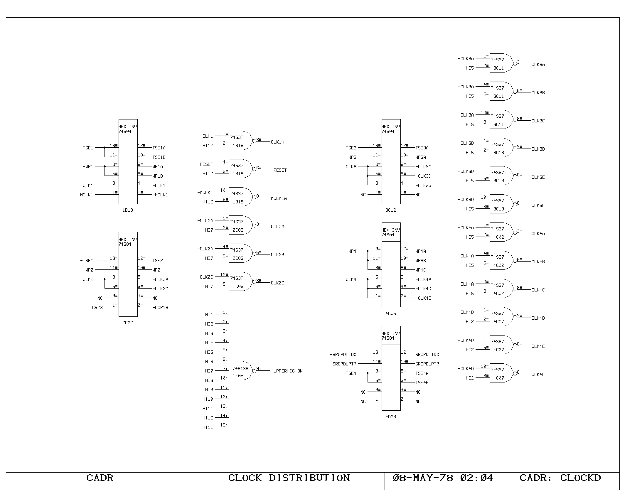
Buffering and gating of the main clock signals is done on the CLOCK2
print. The TPCLK and TPWP flip flop outputs are gated with the
MACHRUN signal (processor running) to produce the final processor
clock and write pulse. These are buffered once here in the clock
circuitry, and once again local to their use in the processor, as
shown in the CLOCKD print.
Two other timing signals are generated from the main timing chain.
TPWPIRAM is used to produce a slightly wider and earlier write pulse
for the control memory rams. TPTSE is a signal generated during the
very first part of each processor cycle which disables all tristate
drivers on the M and A busses, preventing noise problems due to
tristate enable overlaps caused by instruction decoding skews.
The choice of a delay line clock generator rather than a totally
synchronous crystal oscillator generator was based on a desire to
allow the processor to “hang” waiting for a main memory response, and
then immediately resume when the data was available. With a totally
synchronous design, the delay before the available data could be used
might be quite high due to synchronizer problems and quantization of
time in units of the fastest oscillator interval.
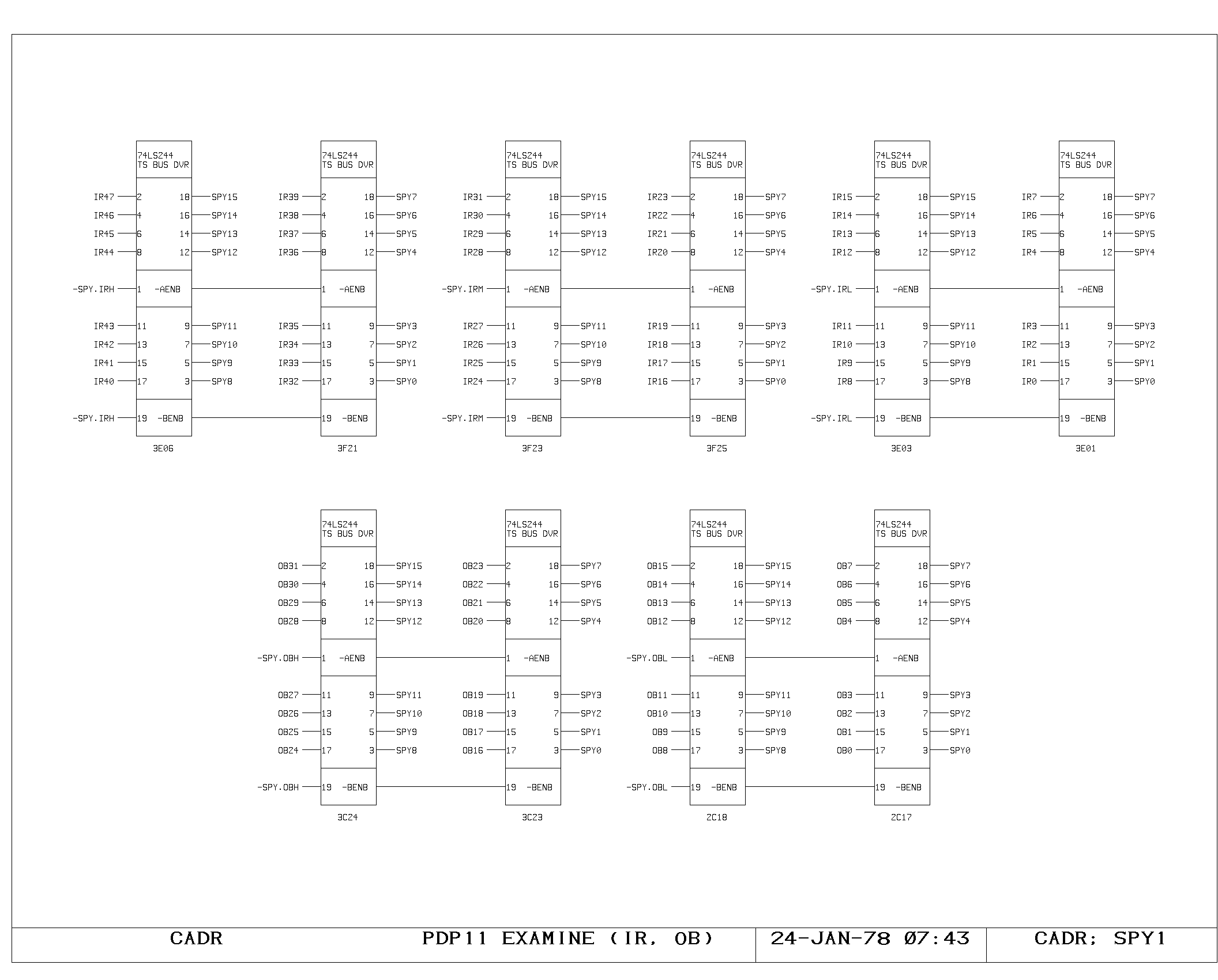
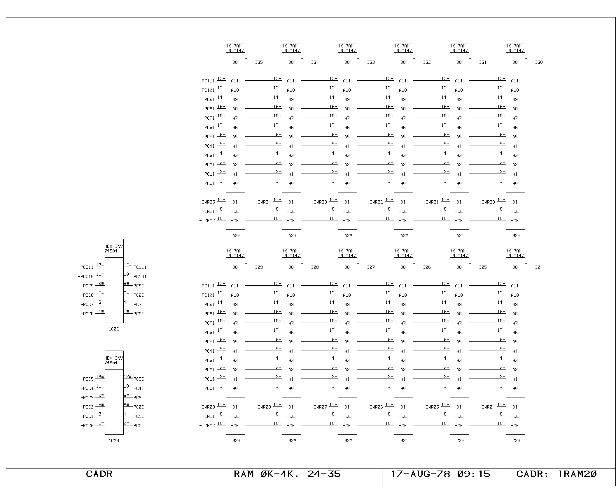
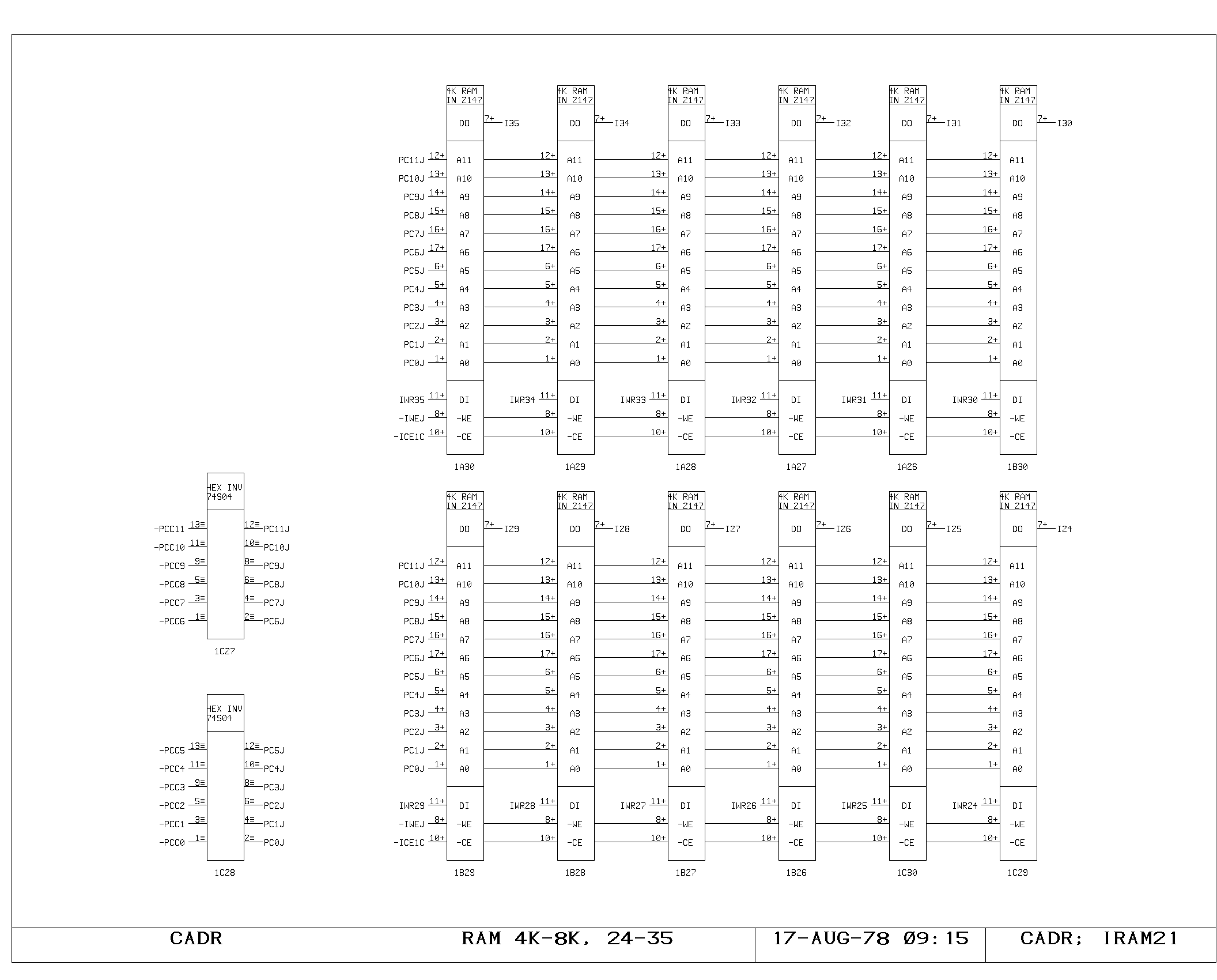
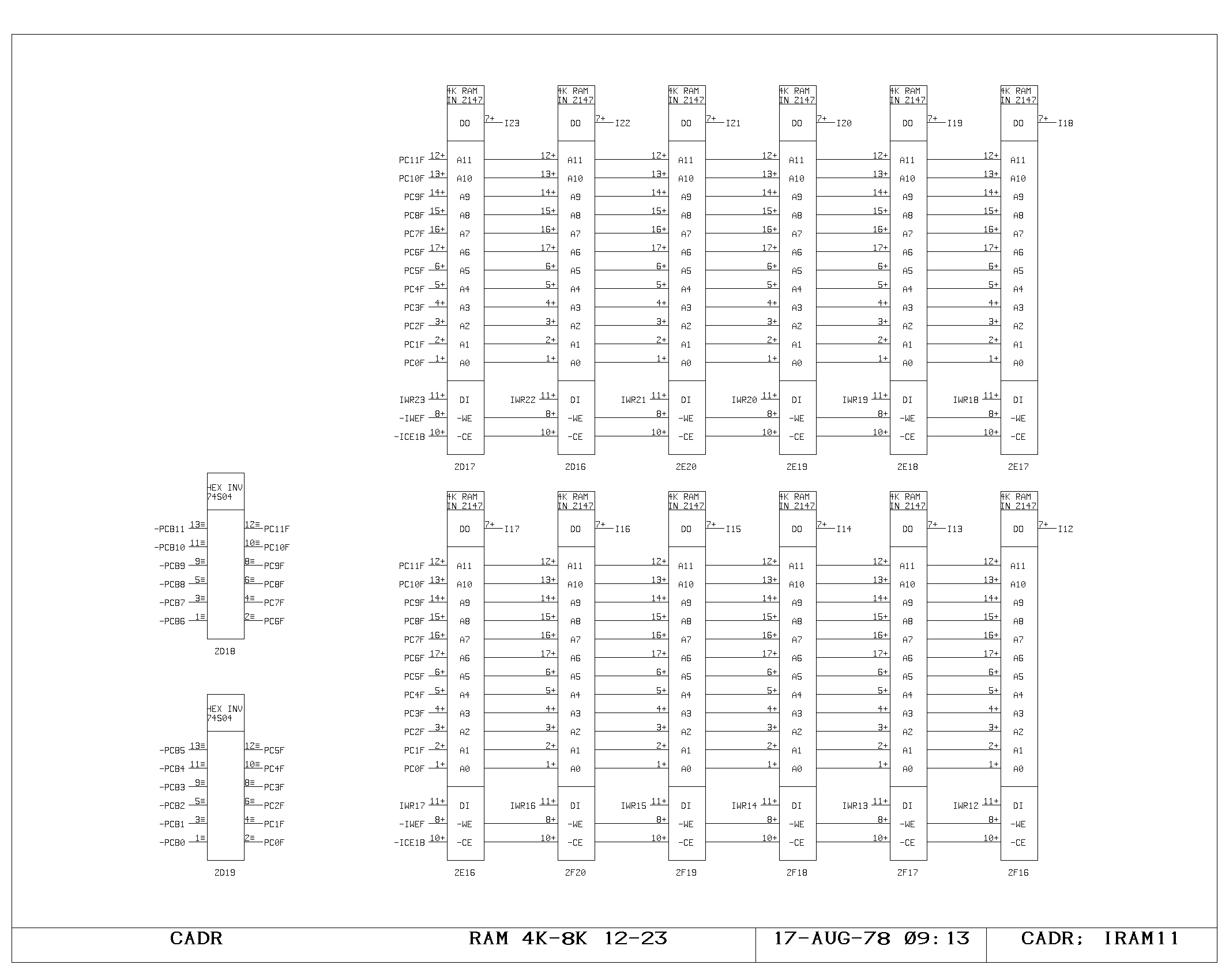
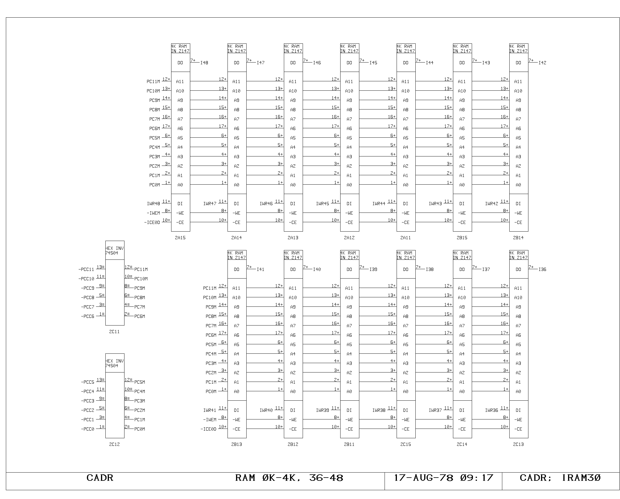
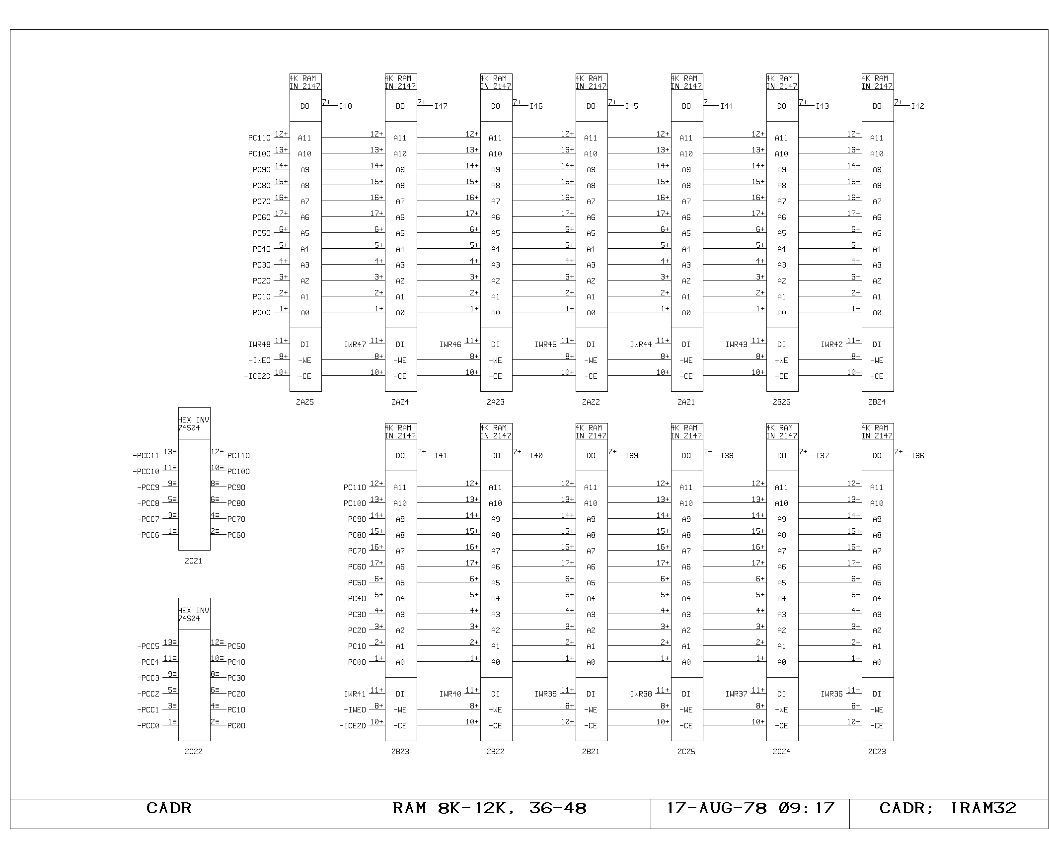
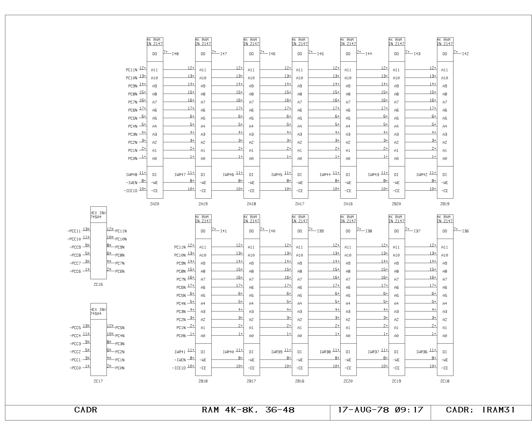
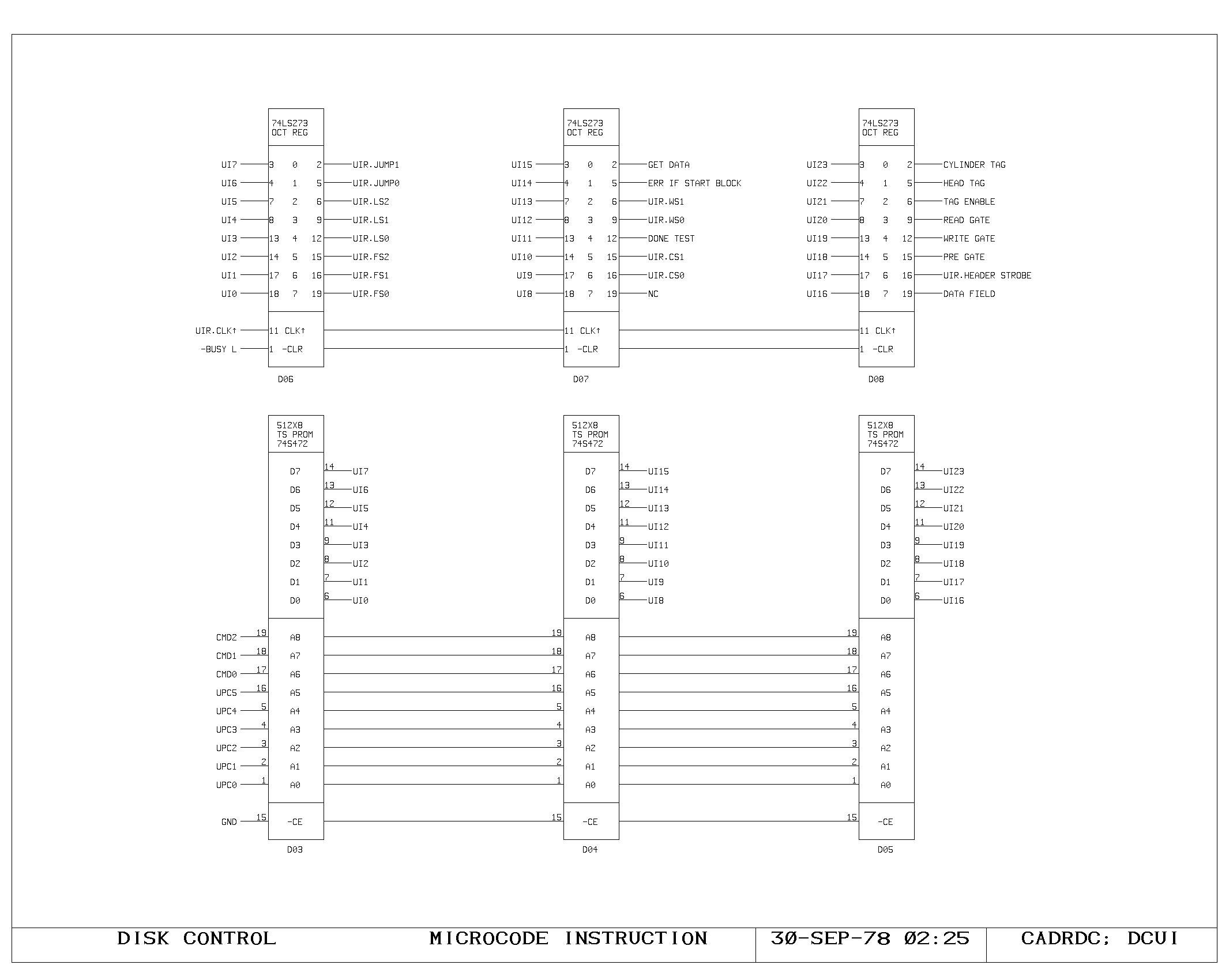
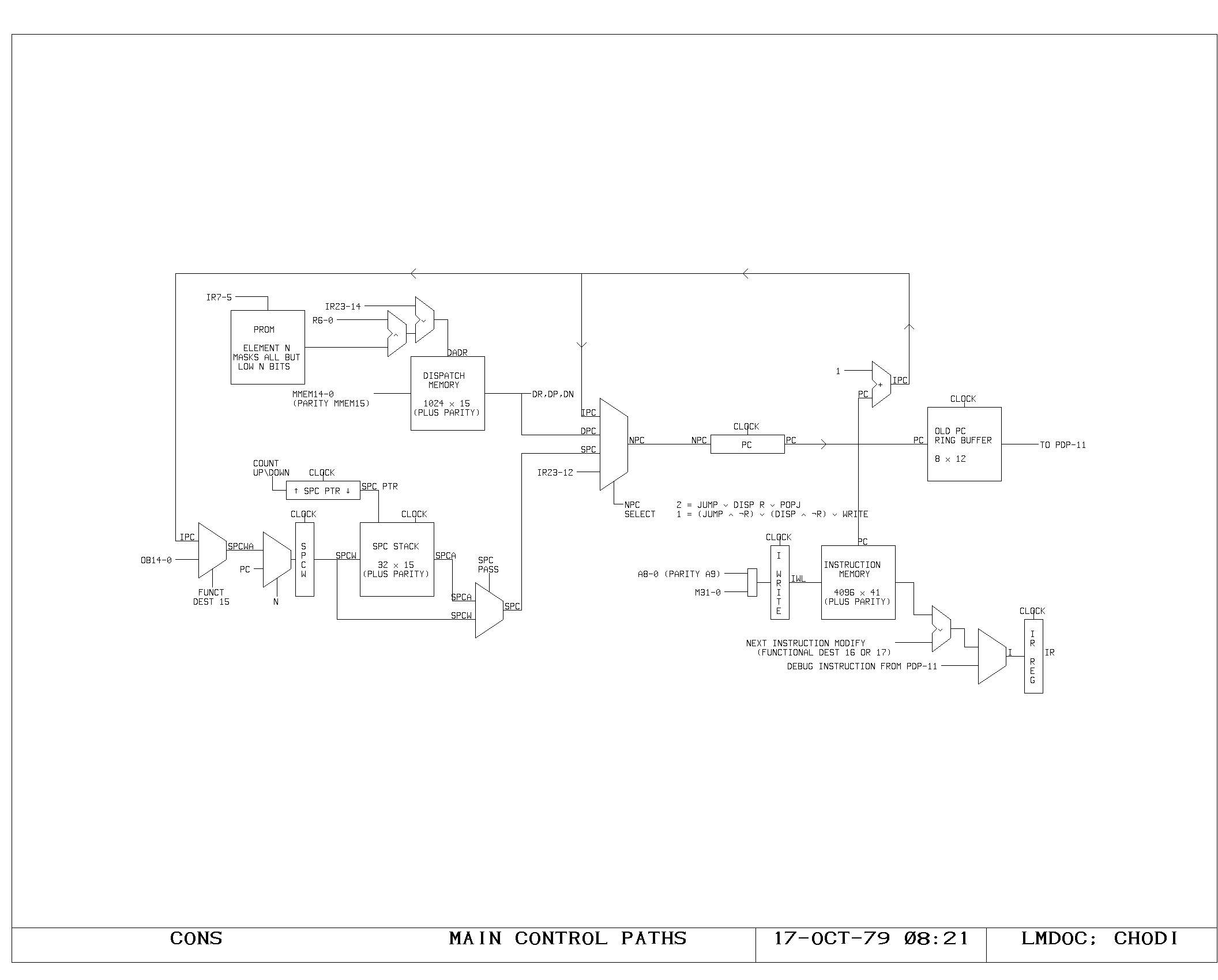
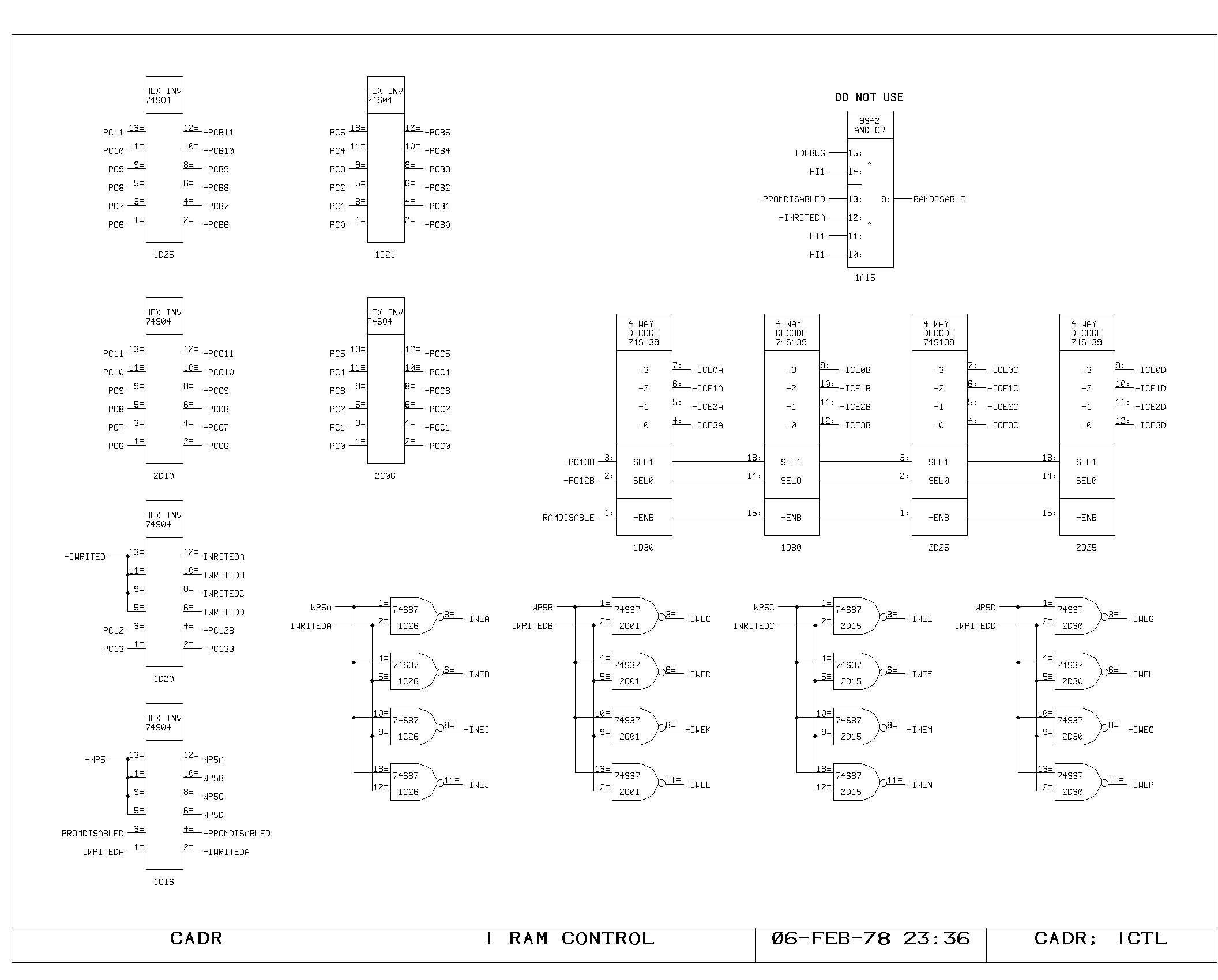
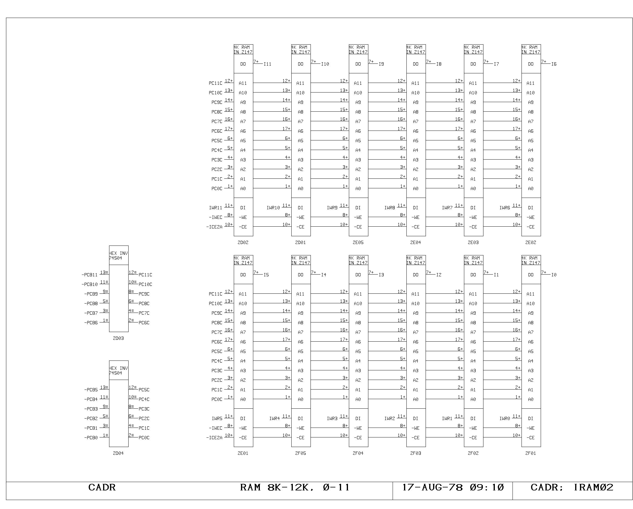
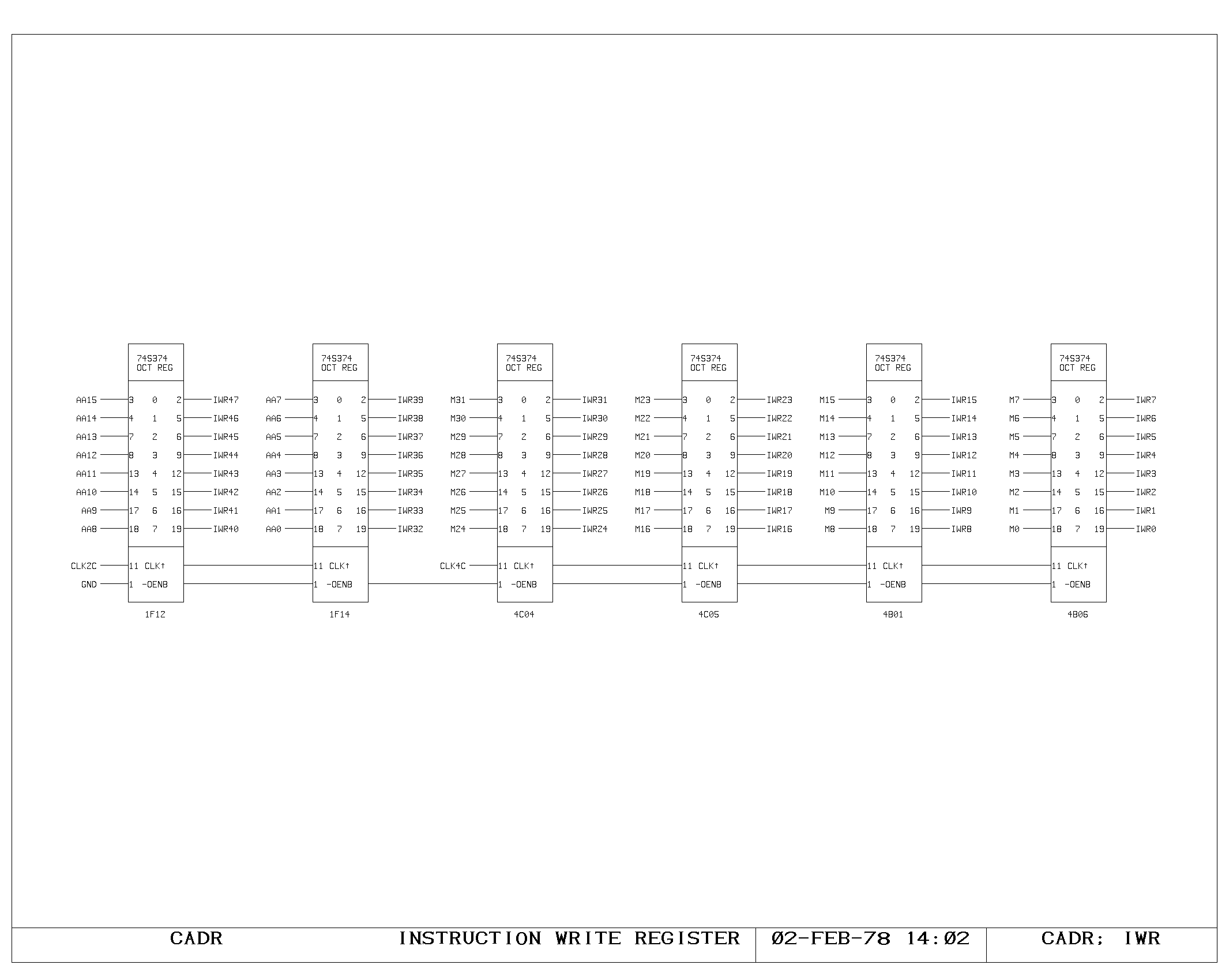
Microinstruction Fetch
During each microcycle, the fetch of the next microinstruction to be
executed is taking place. The PC contains the address of this next
microinstruction. The ICTL print shows the decoding and initial
buffering of the PC for driving the control memory address lines. A
portion of the control memory itself is shown on the IRAM00 through
IRAM03 prints. The microinstruction fetched is 49 bits wide, including
the parity bit. The IWR print shows the register used to hold data
which is about to be written into control memory (the A and M bus data
from the control memory write instruction). The control memory write
pulses are produced and buffered as shown on the ICTL print,
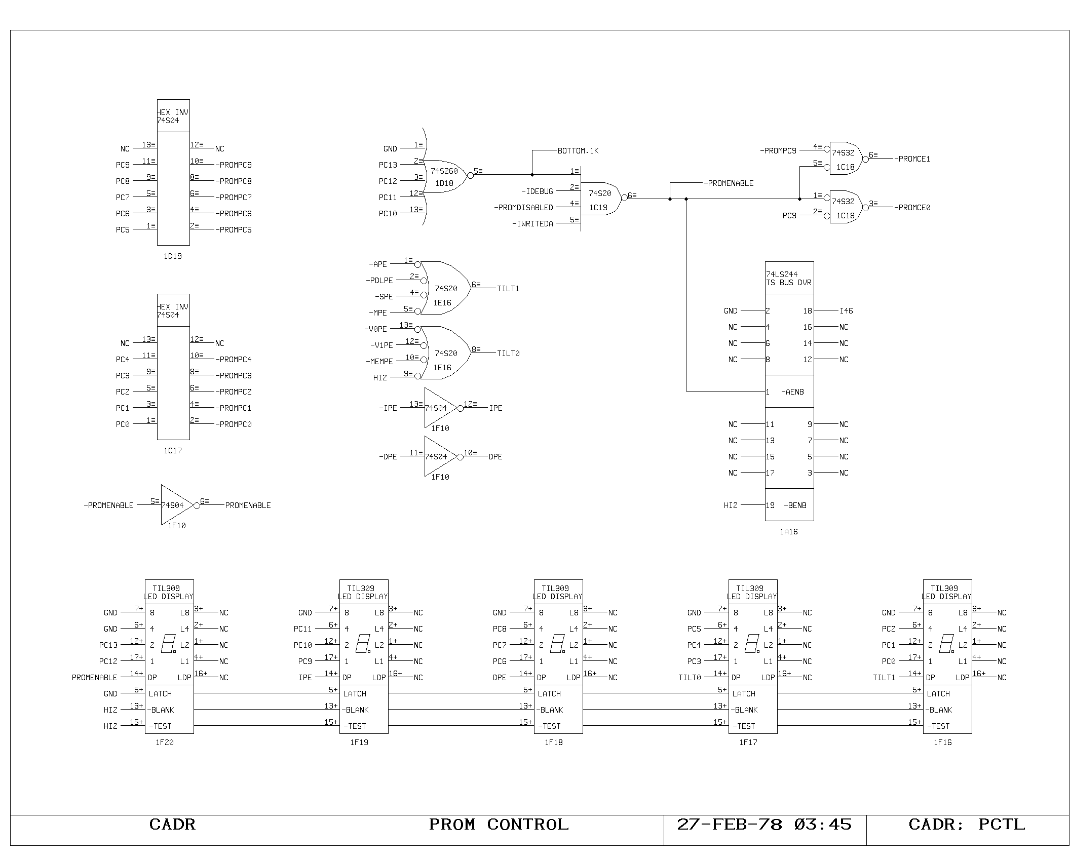
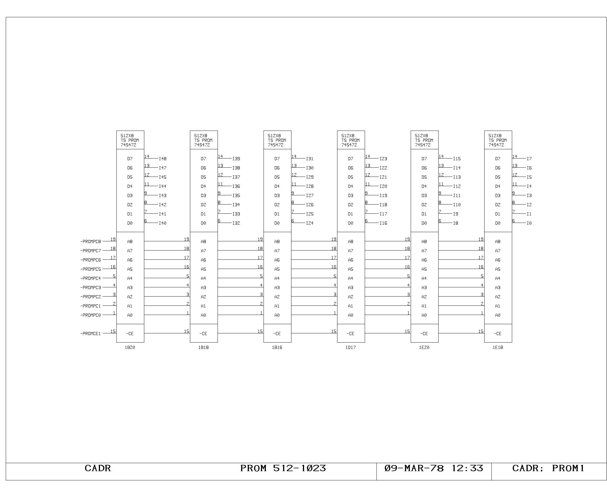
Two other sources of microinstructions exist. The first is the
permanent PROM control memory, which is normally only active during
the processor initial bootstrap. It is 1K by 48, the additional bit
being forced to zero. The address buffering and enable logic is shown
on the PCTL print, while the proms themselves are shown on the PROM0
and PROM1 prints.
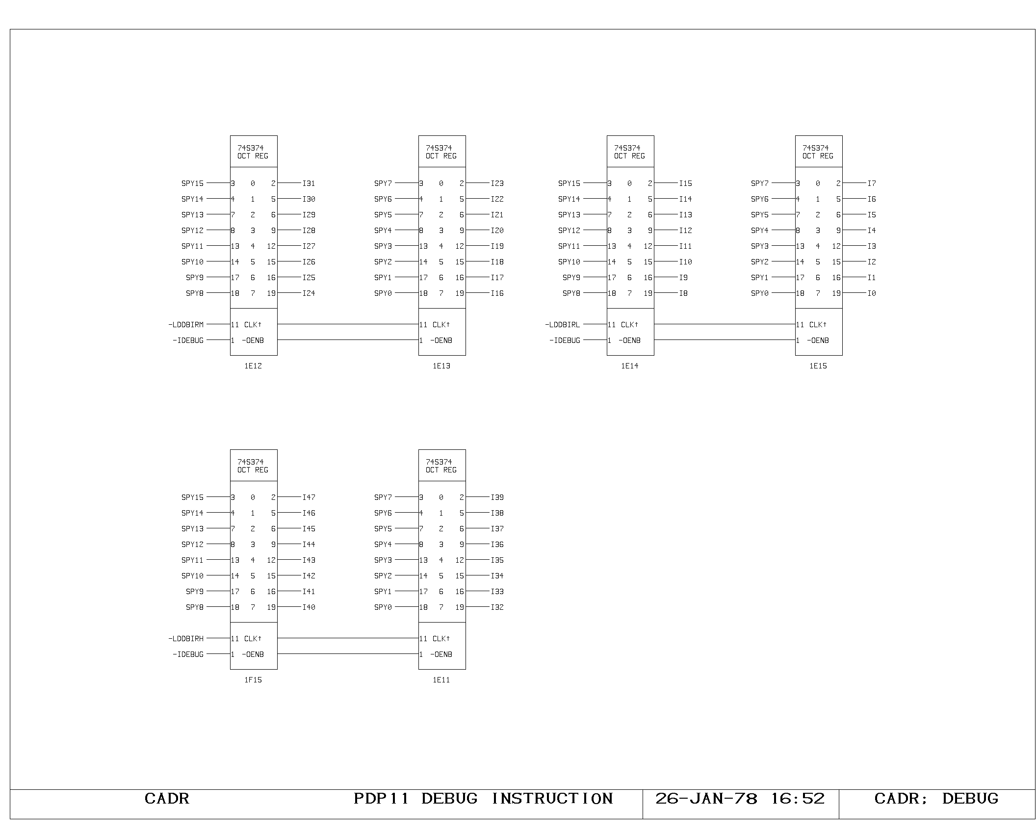
The second additional source of microinstructions is from a register
loadable from the console computer interface. This source allows the
debugging computer to execute arbitrary instructions on the processor,
exercising its datapaths, and allowing access to internal processor
state which is not directly readable through other console computer
paths. The execution of microinstructions through this path is the
main mechanism by which the console computer exerts control over the
processor.


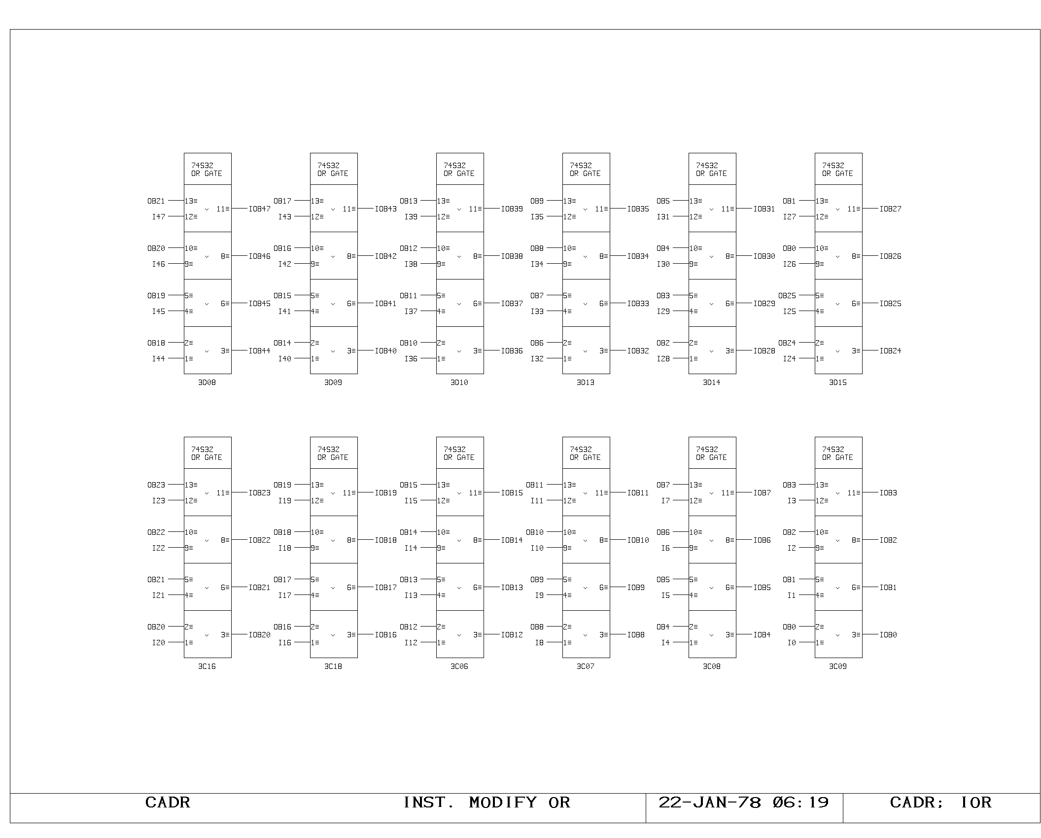
Microinstrction Modification and Main Instruction Register
The fetched microinstruction word can potentially be modified by the
result of the previously executed microinstruction. This is
implemented on the IOR print by inclusively ORing the main output bus
(OBx) with the output of control memory (Ixx) to produce the IOBxx
modified signals. The main processor instruction register on the IREG
print conditionally selects either the modified or unmodified result,
depending upon whether the instruction modification feature has been
activated. The clocking of a new instruction into the IR register
marks the initiation of execution for the new microinstruction.

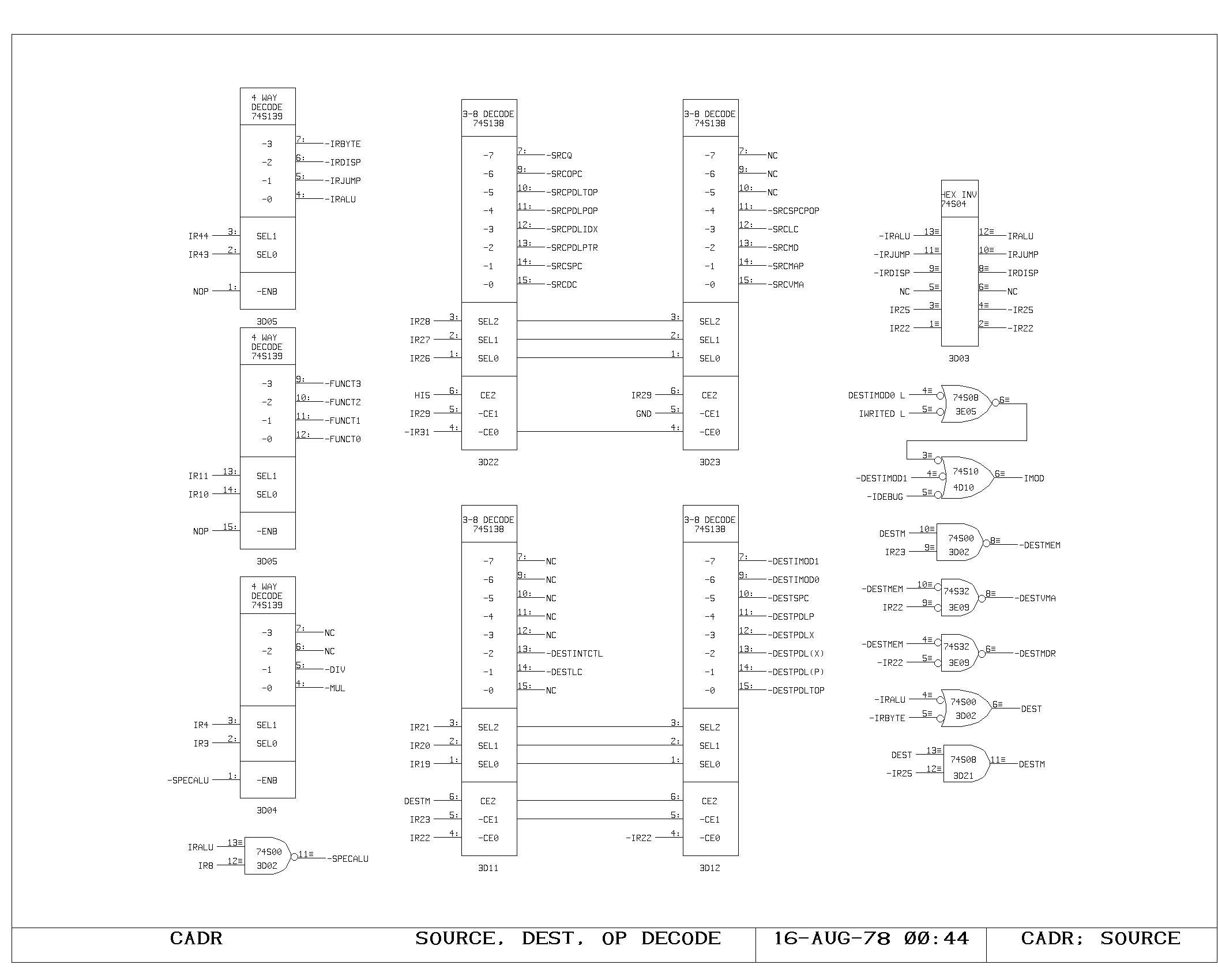
IR Decoding
For the most part, the processor is designed so that the initial phase
of microinstruction execution is independent of the details of the
particular instruction. The decoding of the IR fields, then, as shown
on the SOURCE print is not in the critical path of cycle timing.

The four main instructions are decoded from a pair of IR bits,
providing the IRBYTE, IRALU, IRJUMP and IRDISP conditions. All of
these are inhibited if the execution of this cycle is NOP’d.

The SRCxxx conditions specify a particular source of M bus data. These
are activated only if a normal M memory location is not specified
(IR31 set).

The destination codes are not needed until quite late in a cycle and
are decoded in several stages. First, only the IRBYTE and IRALU
instructions specify destinations, producing the DEST signal. Next,
only destination codes with bit IR25 clear specify an M register
address (less than 32.) producing DESTM. These, of course, also
specify a functional destination, which is decoded from IR19 to
IR22. If IR23 is on, the functional destination is to either the VMA
or MD register, and the memory subroutine further decodes this field.
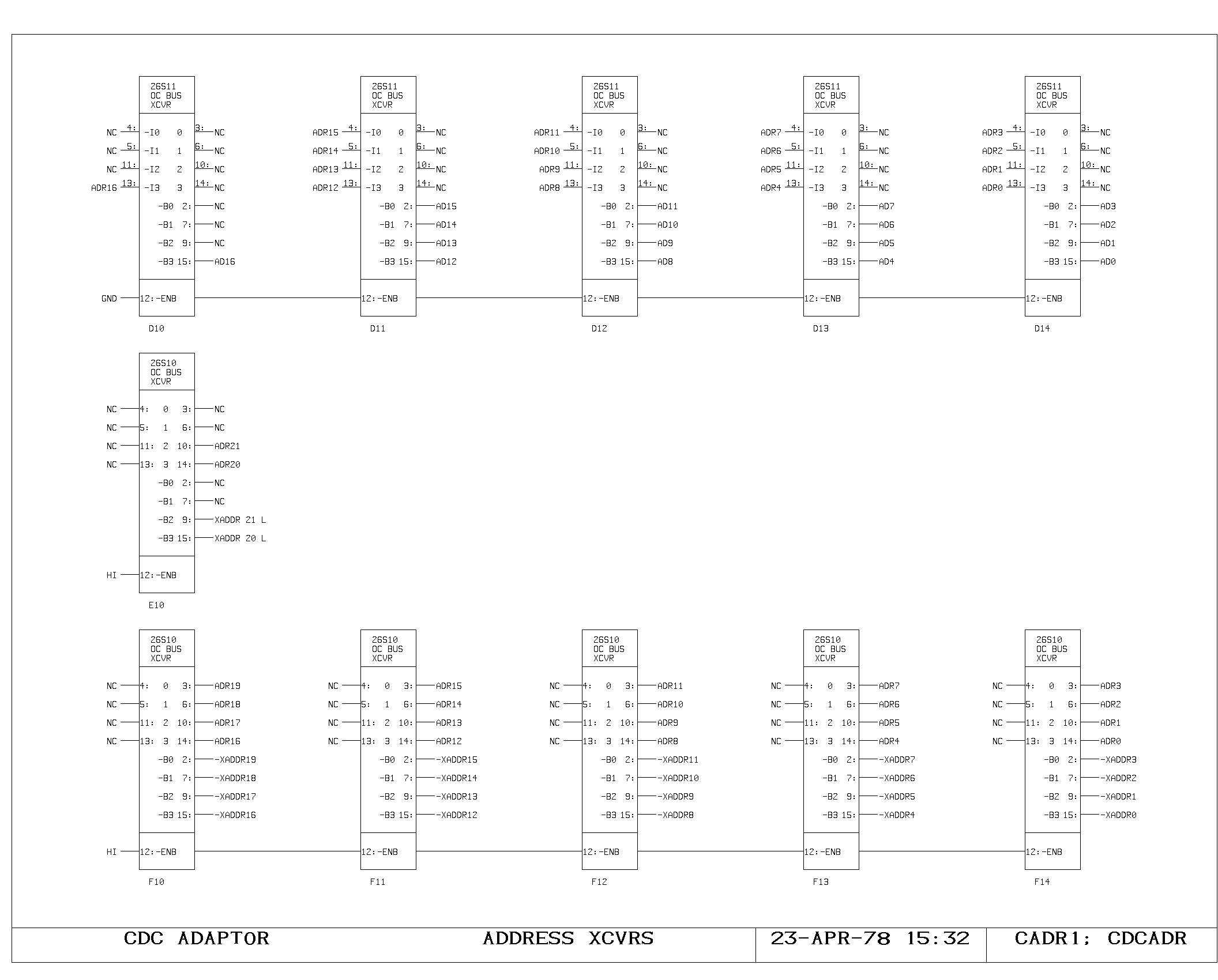
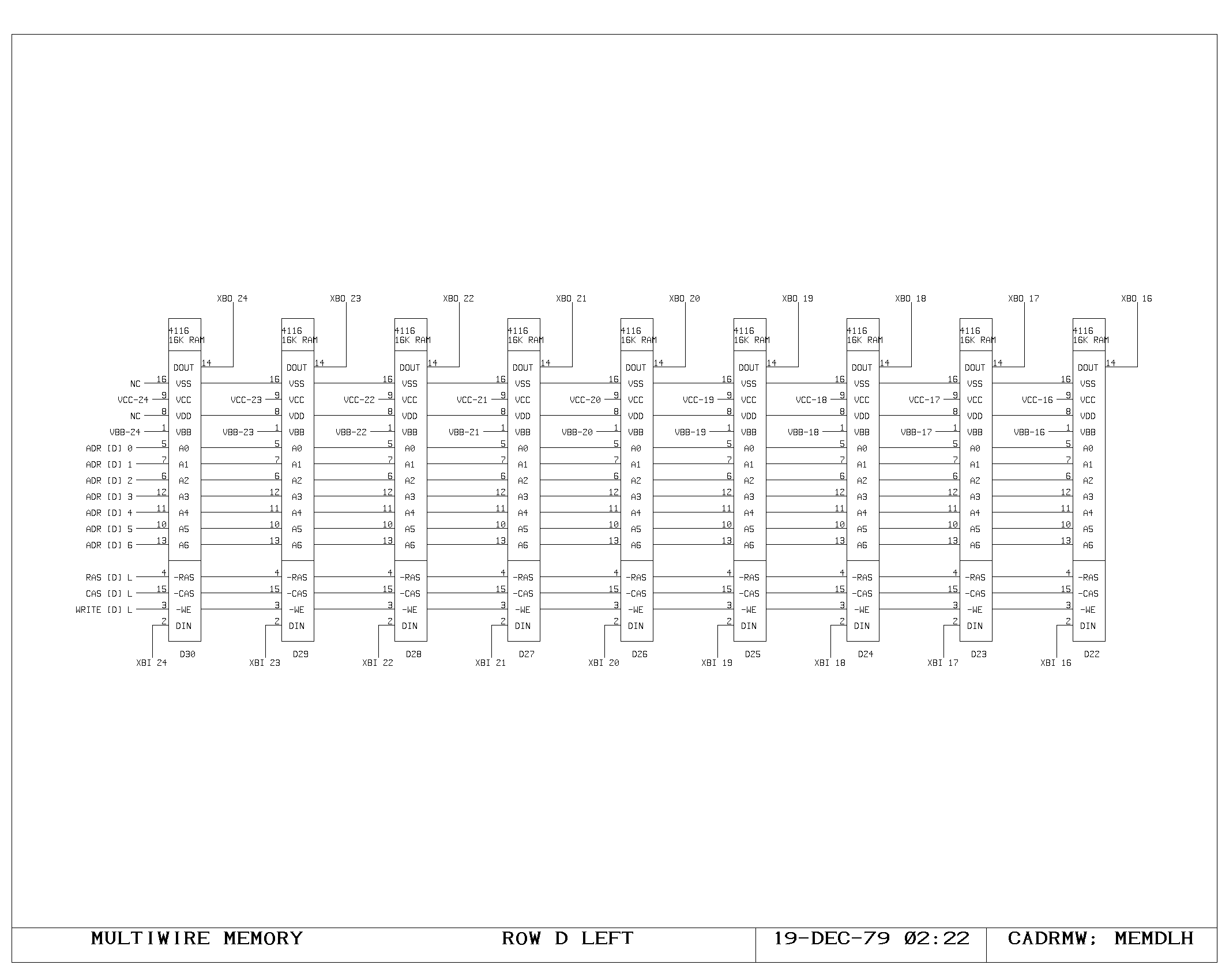
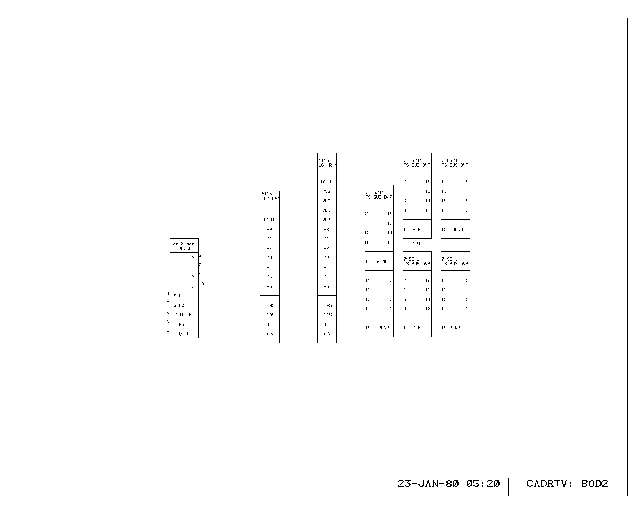
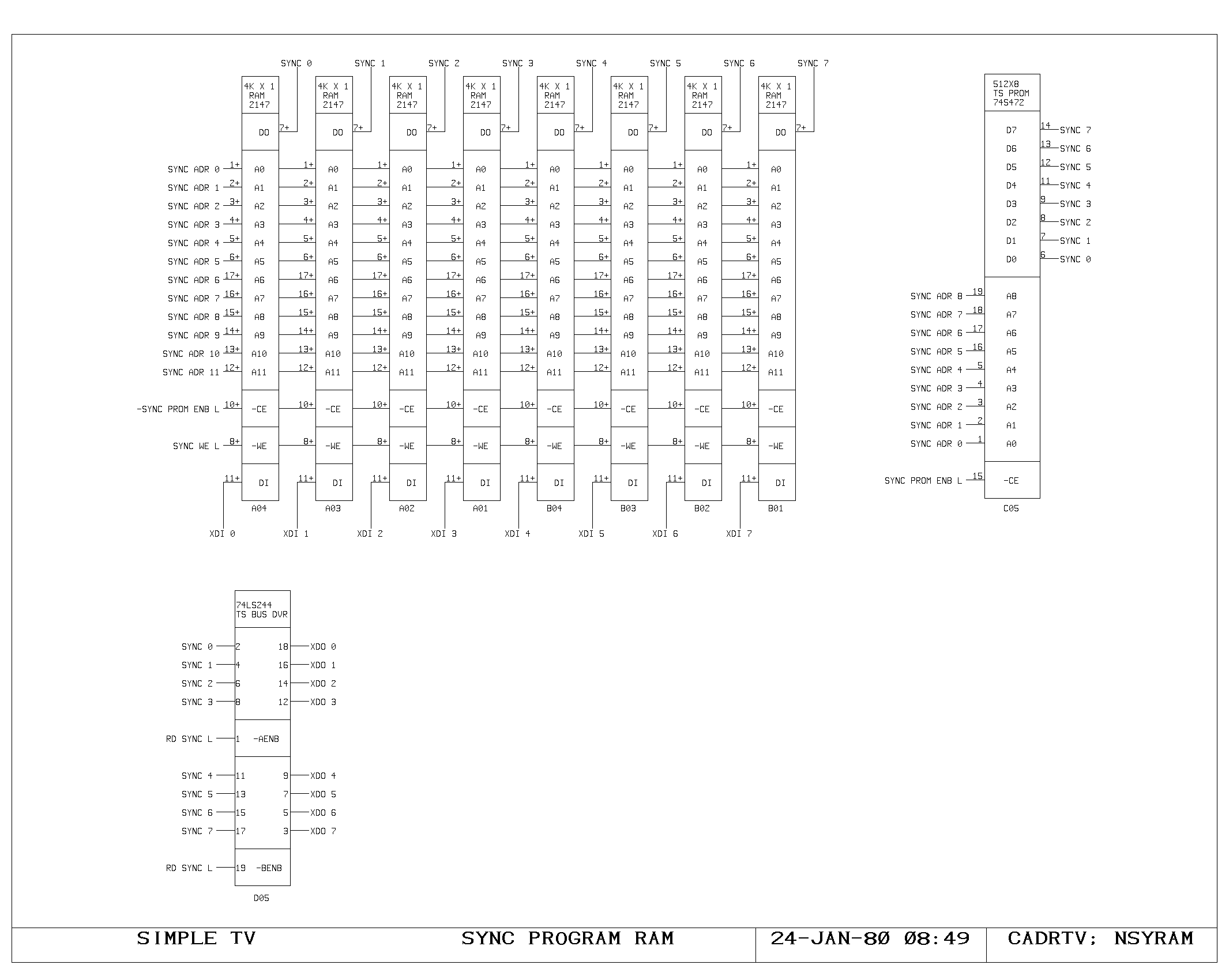
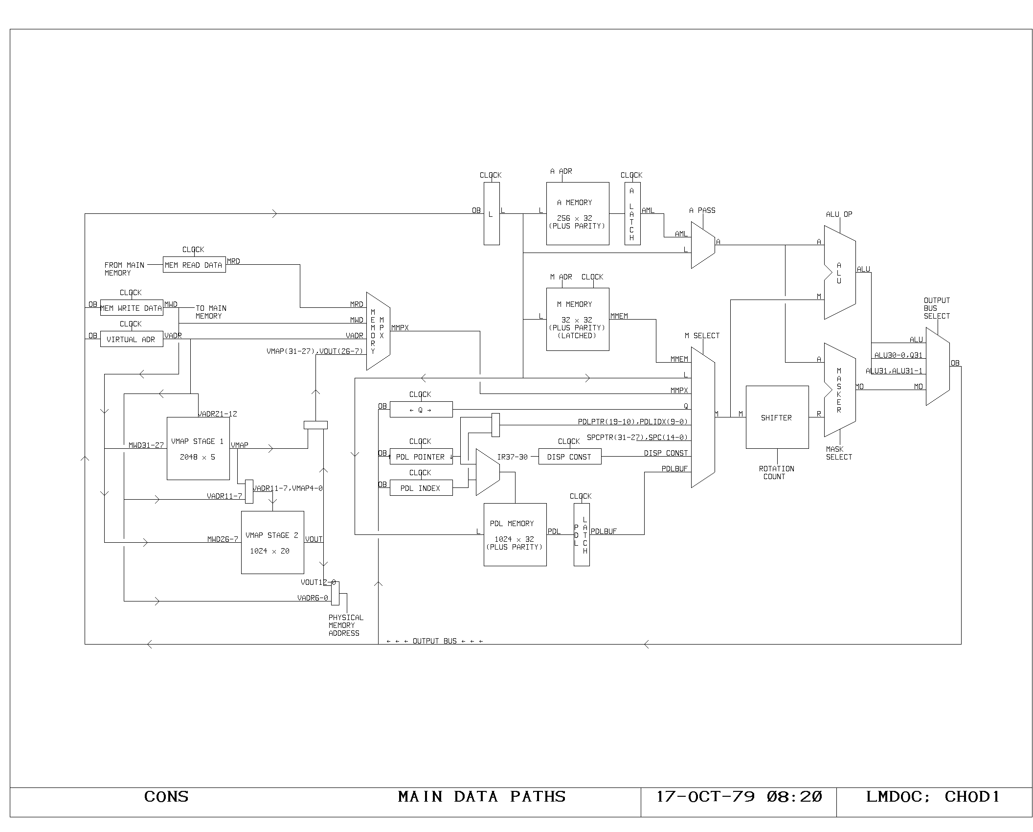
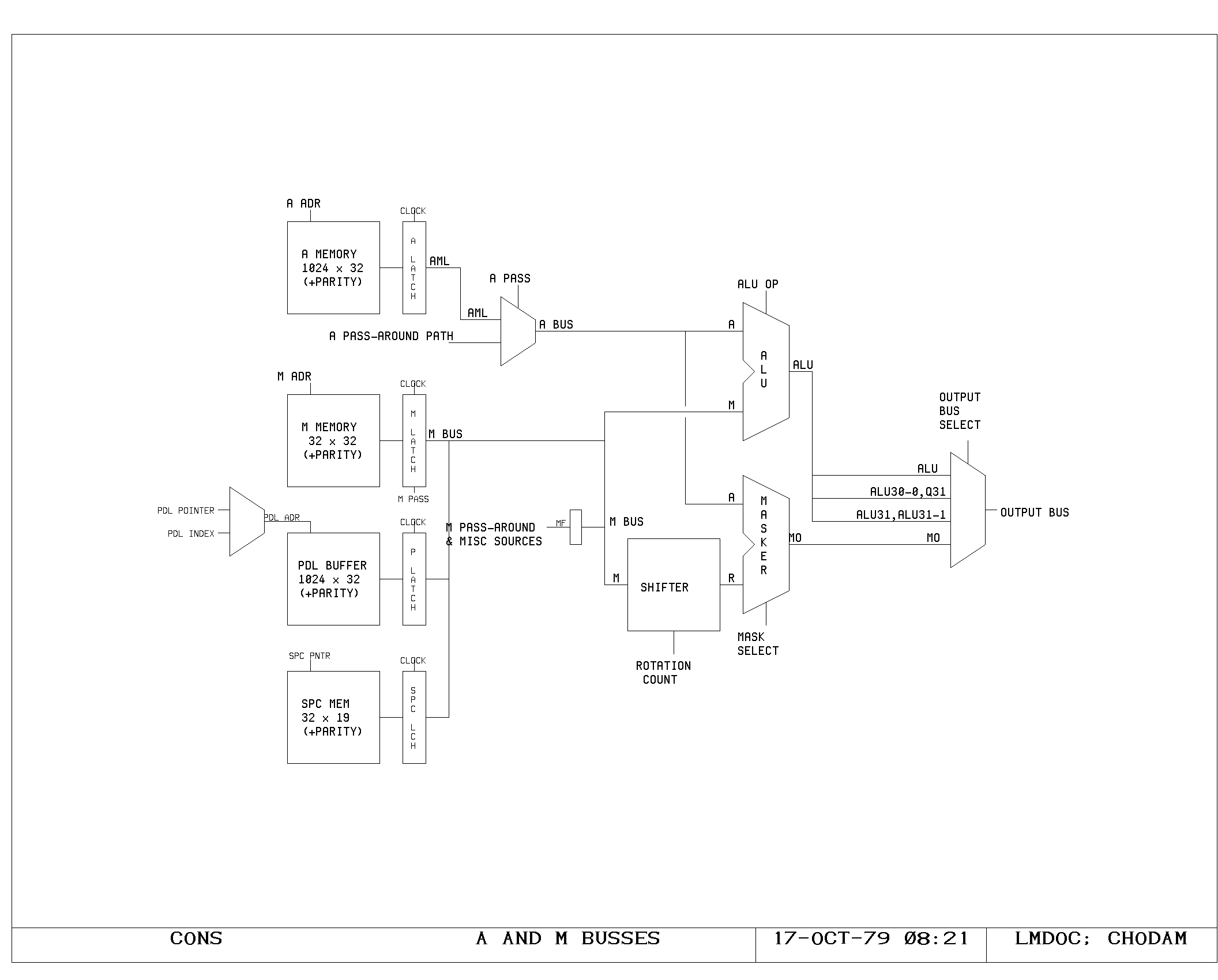
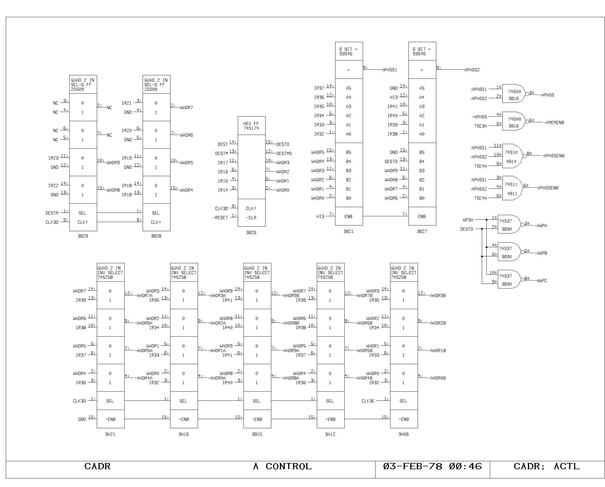
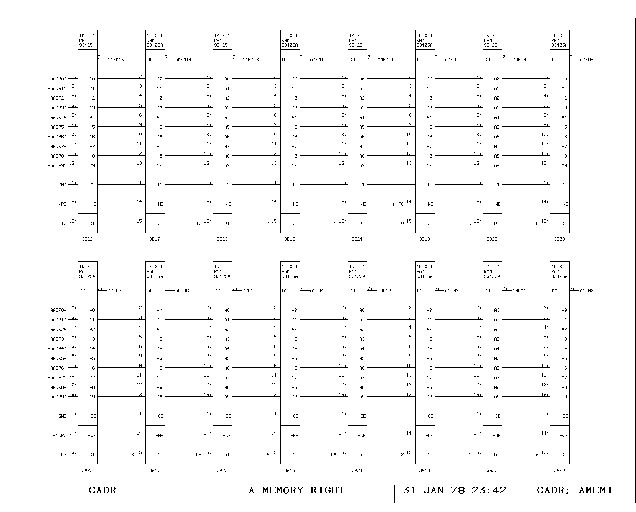
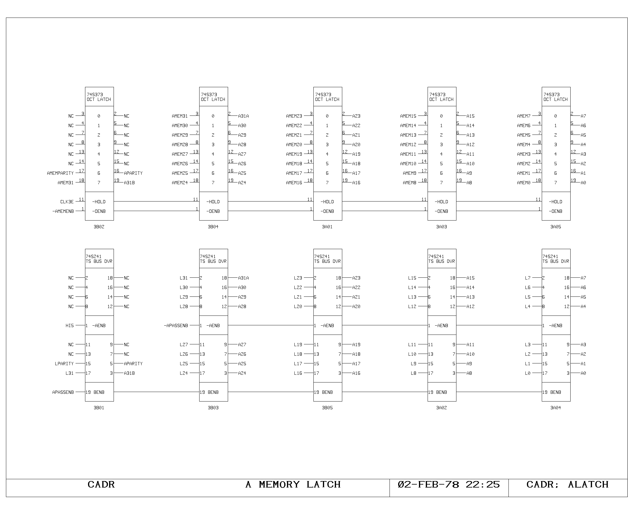
A Memory
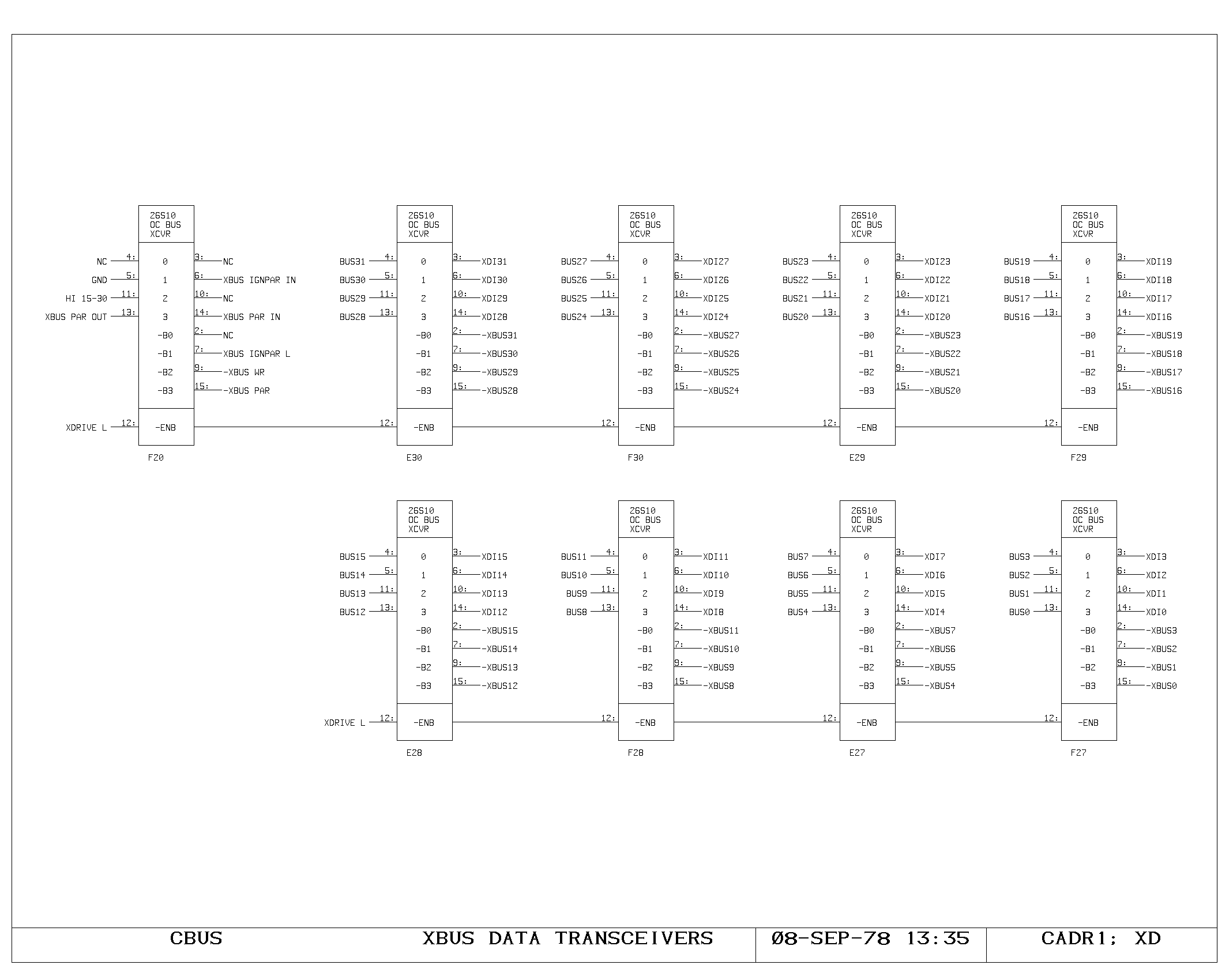
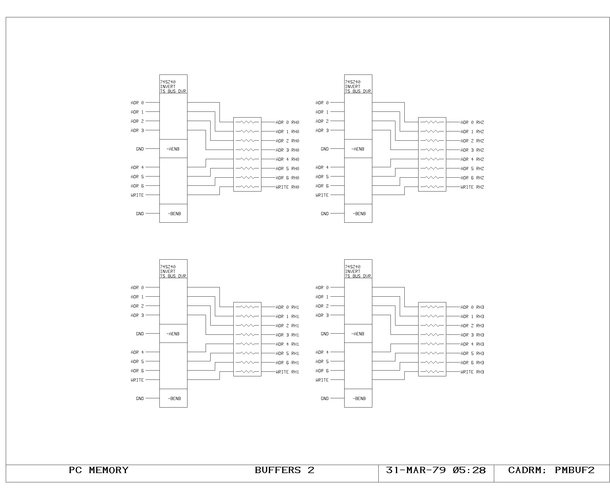
All instructions begin with the fetching of data from the M and A
busses.  Regardless of whether the data will be used, data is fetched
from all of the memories in the machine at the beginning of each
cycle.

In the A memory, the data fetch begins with the high phase of the
clock selecting IR bits 41-32 for driving the A memory address lines
(AADRxx), as shown on the ACTL print. Simultaneously, the A memory
address is compared with the A memory write address from the previous
cycle, in order to detect the situation in which a read is being
performed on a location which has yet to be written. The APASS signal
indicates that this condition has occurred.

After the address access time of the A memory rams (shown on AMEM0 and
AMEM1), the AMEMxx signals are valid at the input of the A memory
latch (print ALATCH).  Either this data or the contents of the L
register (which stores the yet to be written result of the previous
instruction) is driven onto the A bus as determined by the APASS
signal (AMEMENB and APASSENB on ACTL).

When the main clock falls, the A memory latches close, holding the
output of the A memory for the remainder of the cycle. Data from the L
register will of course be valid throughout the cycle.

Simultaneously, the A memory address selector (ACTL) selects the
previous cycle’s write address as the A memory address. If the
previous cycle specified an A memory destination (DEST) then an A
memory write pulse is generated (AWPx) writing the data from the
previous cycle.

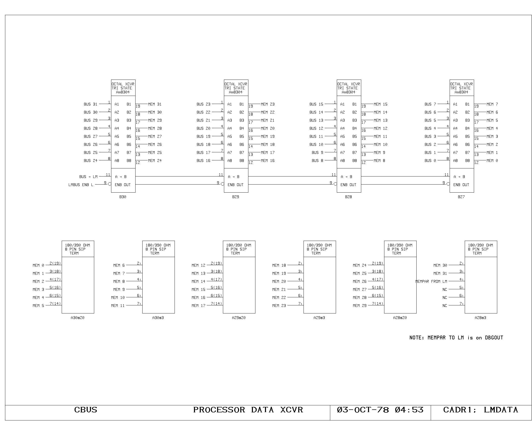
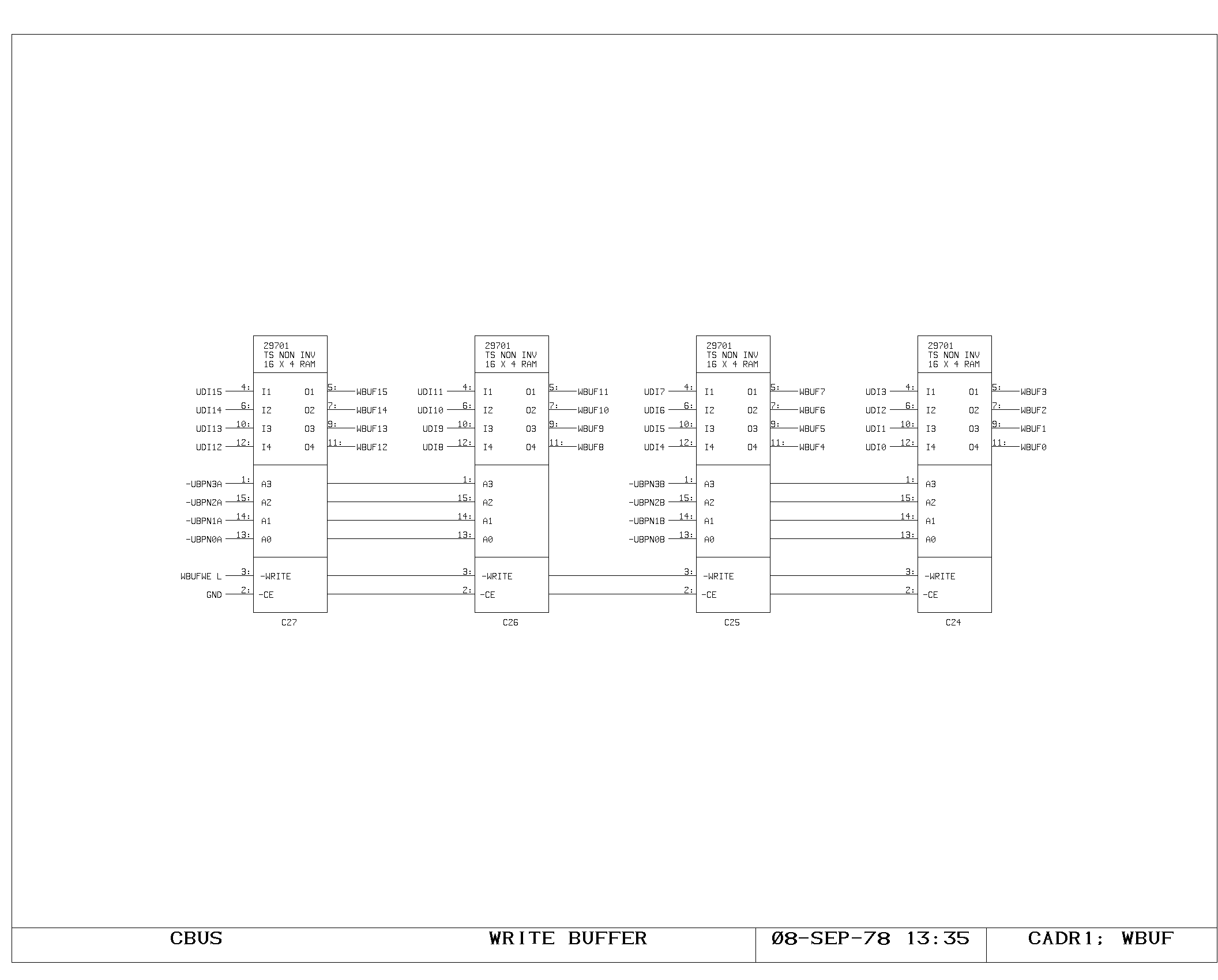
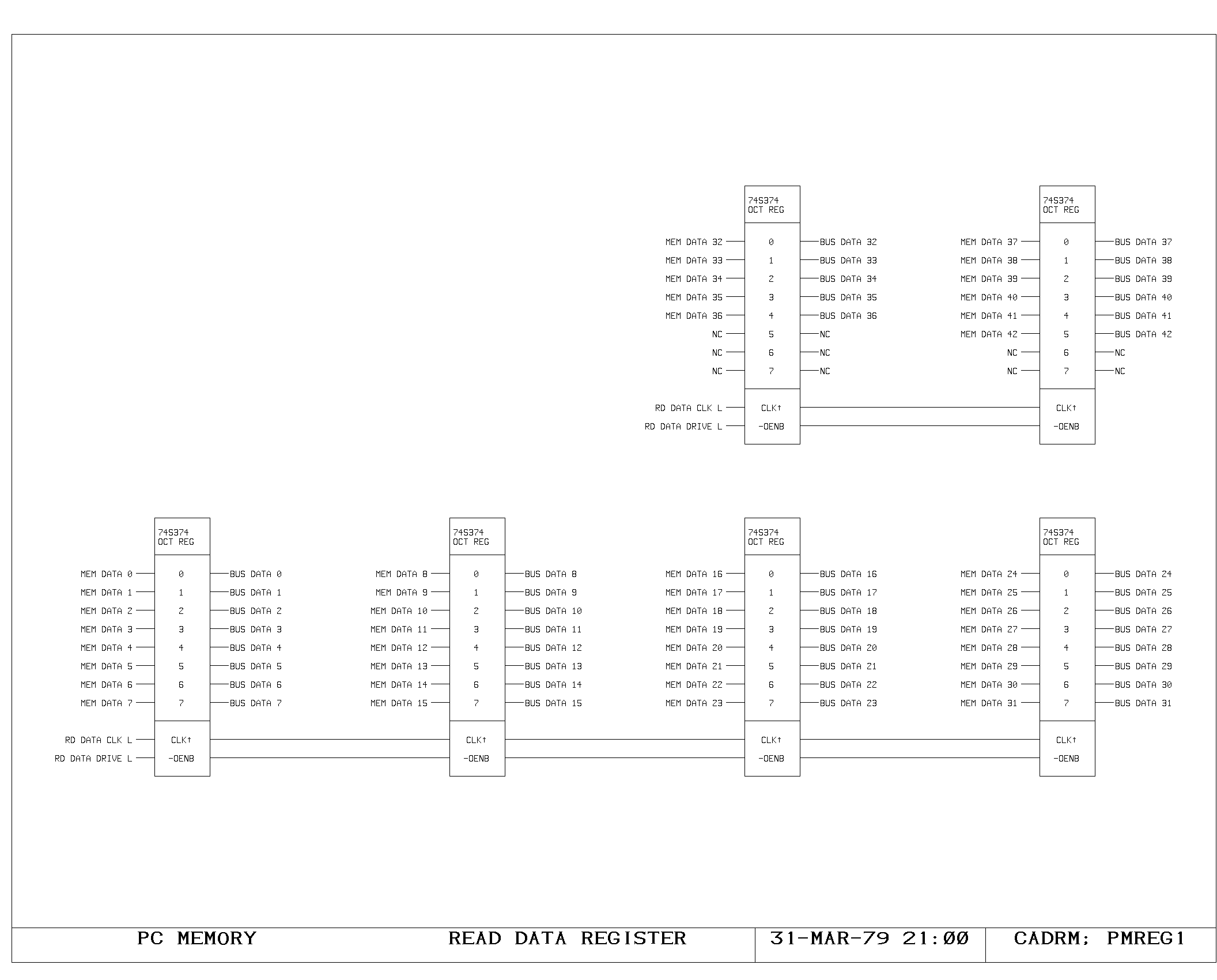
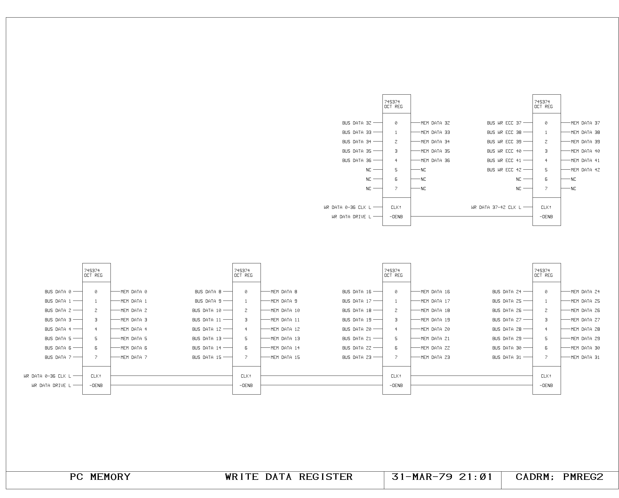
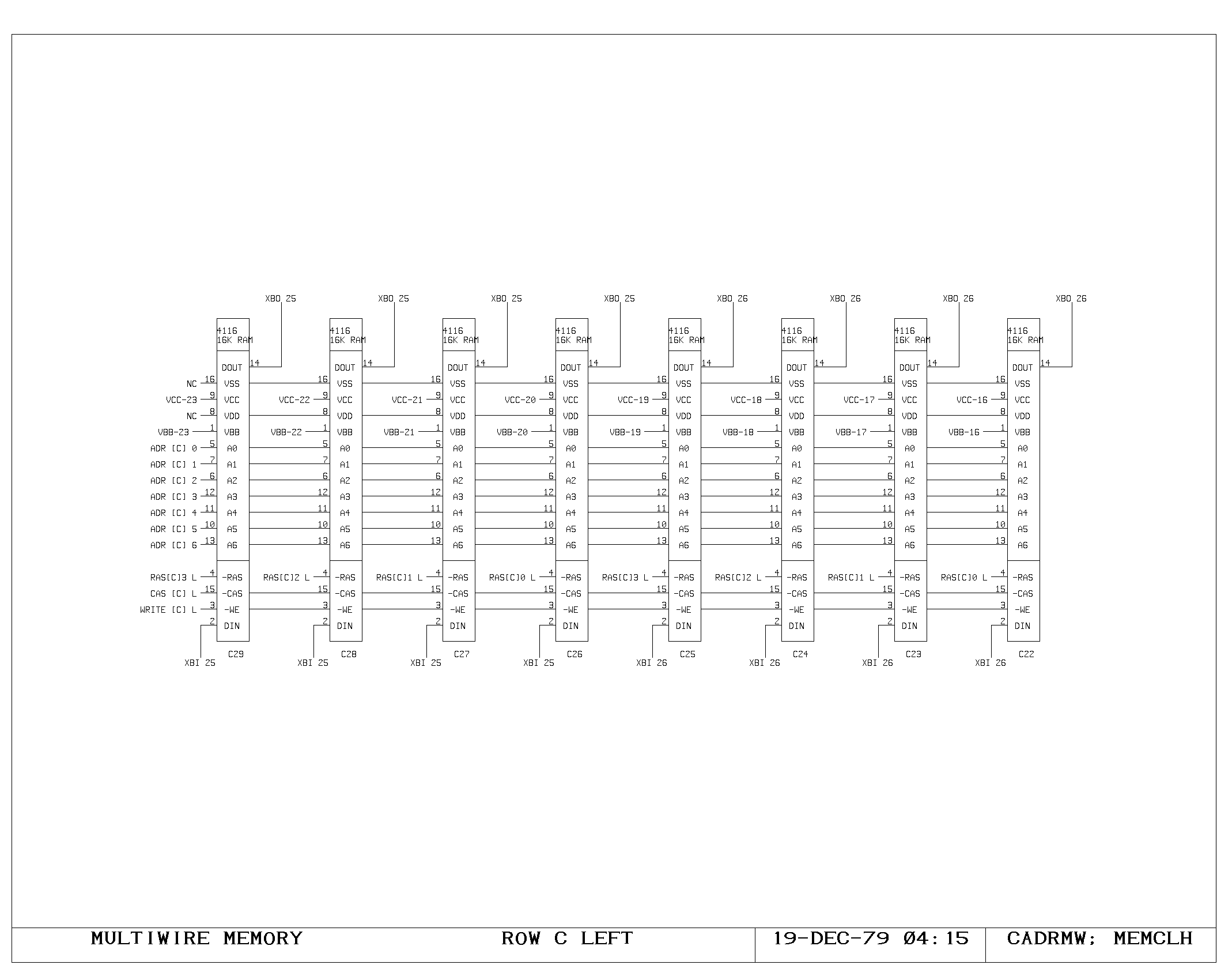
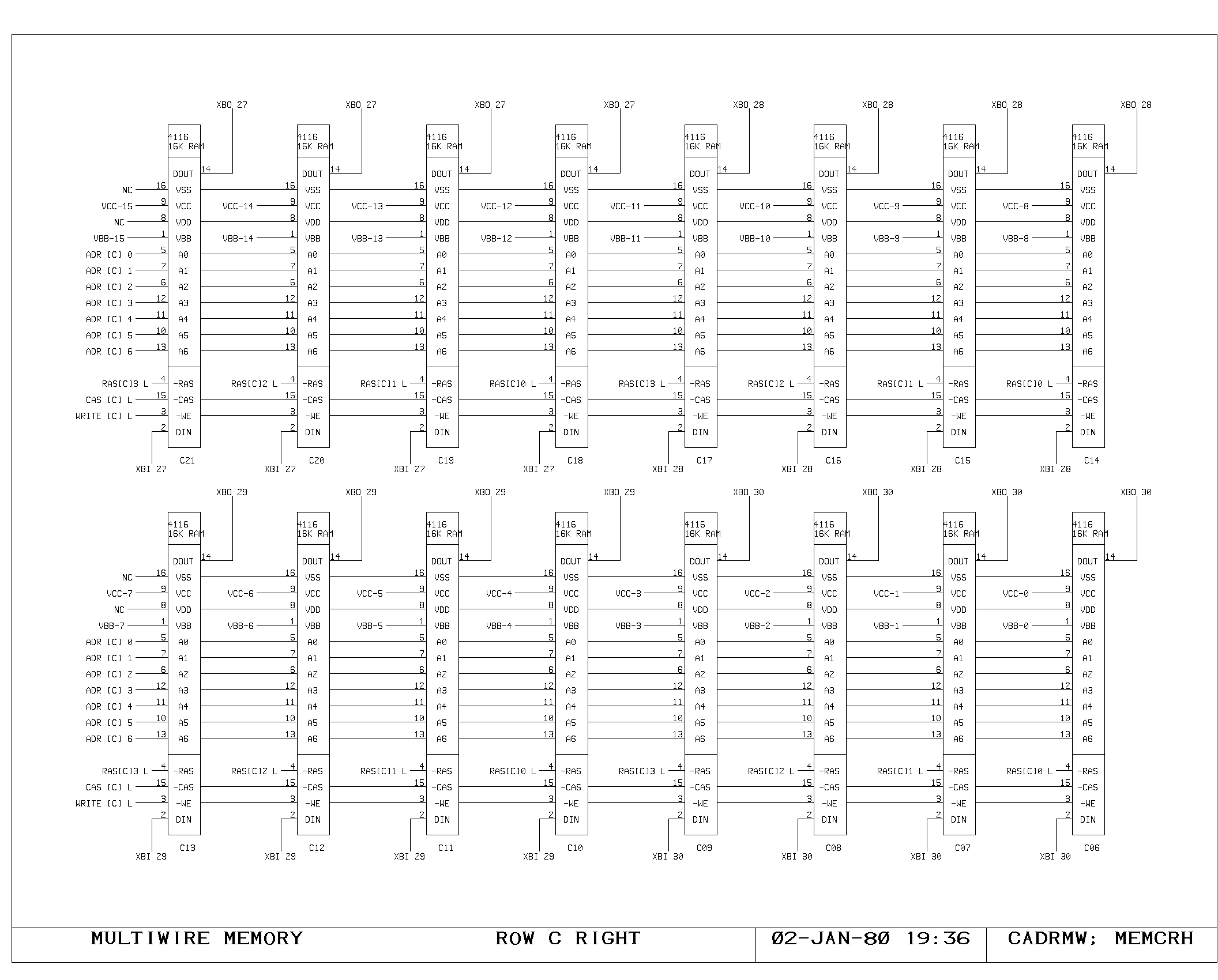
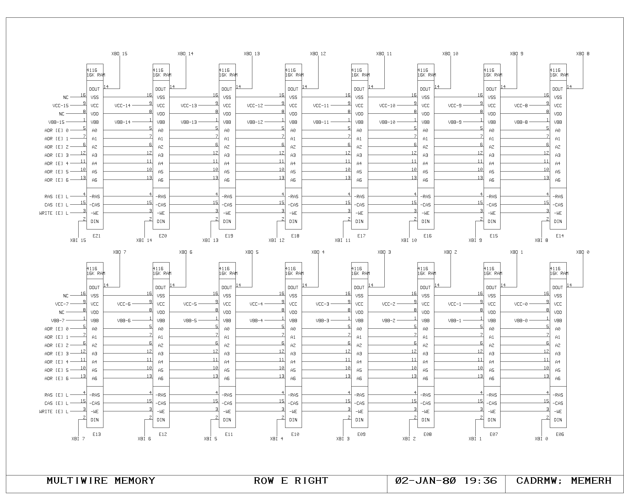
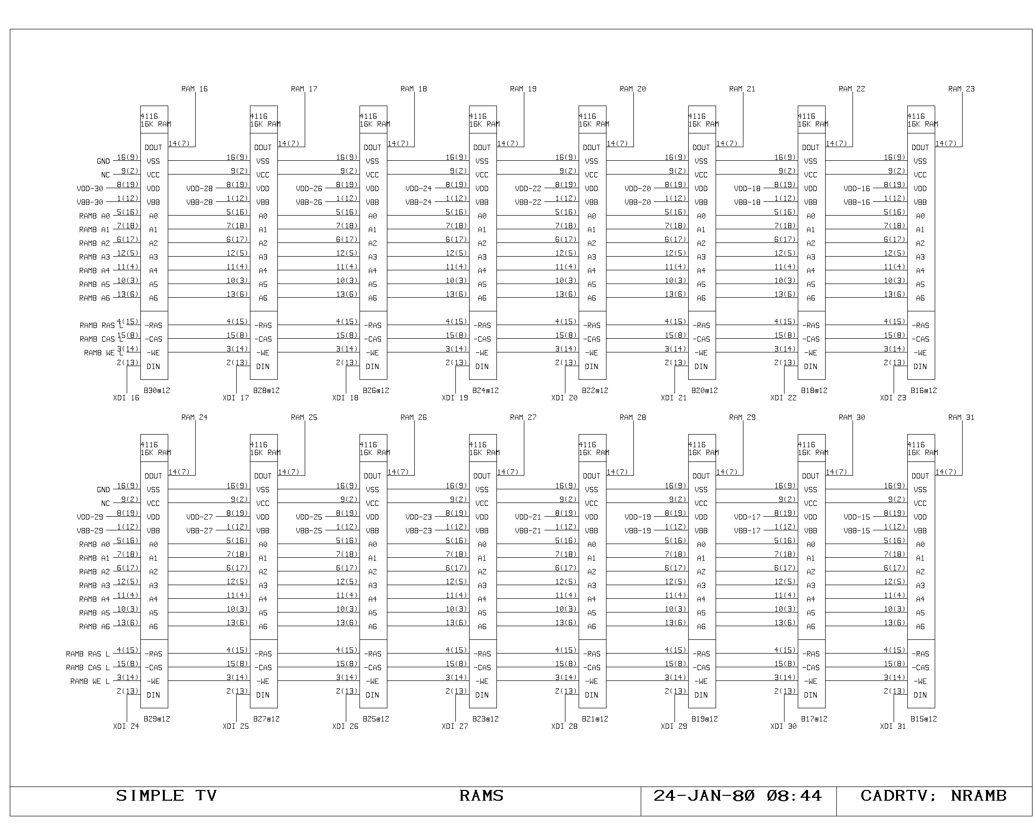
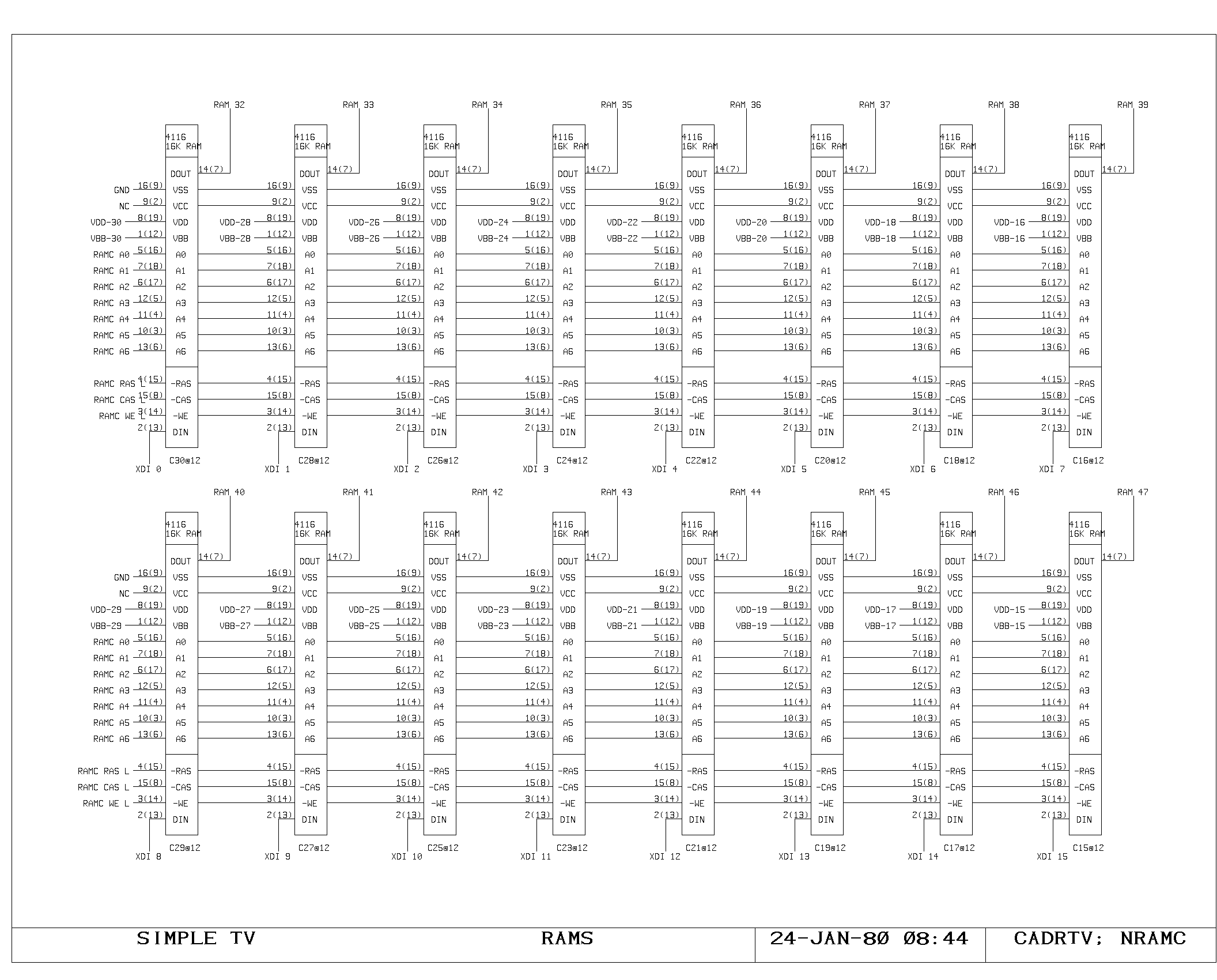
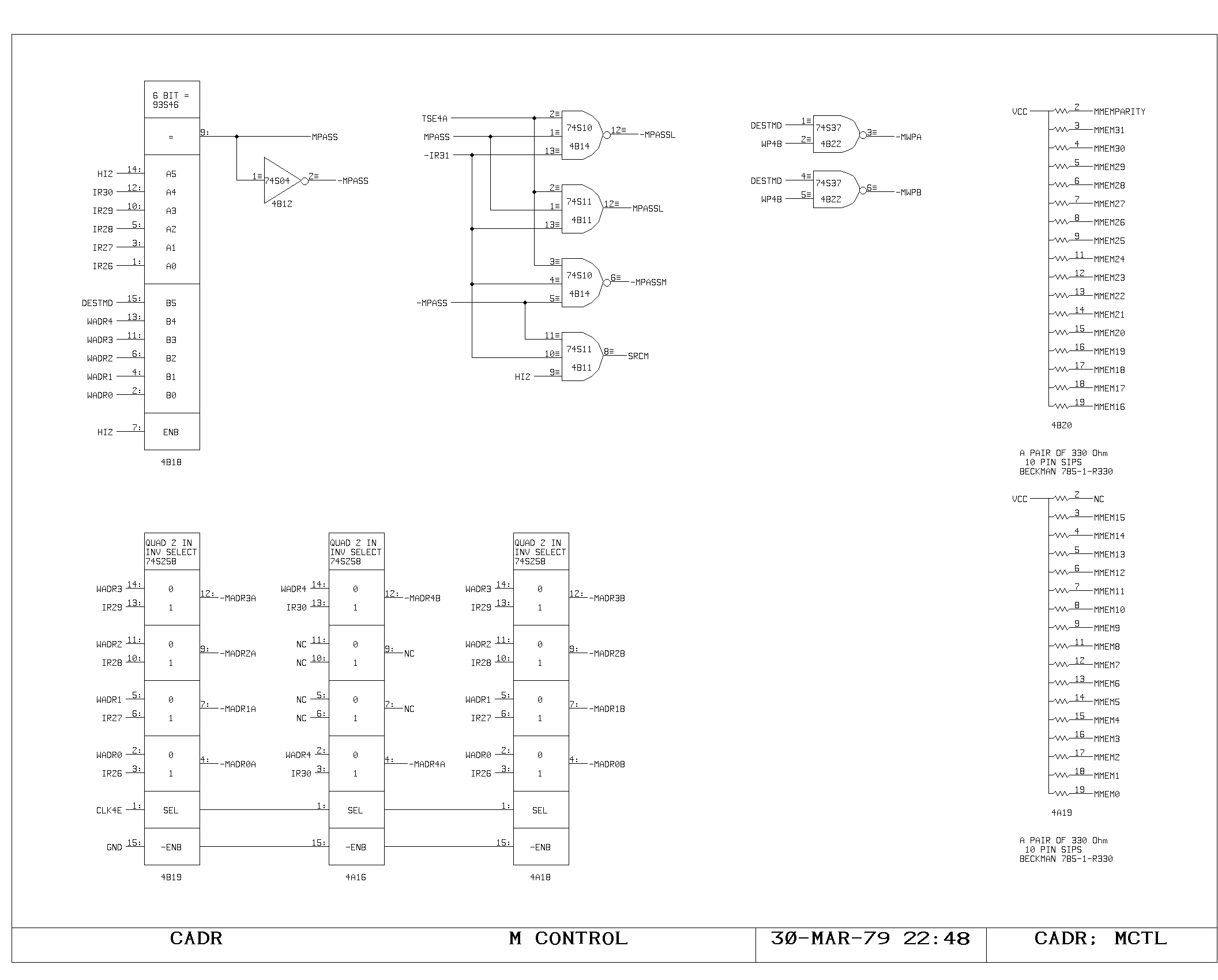
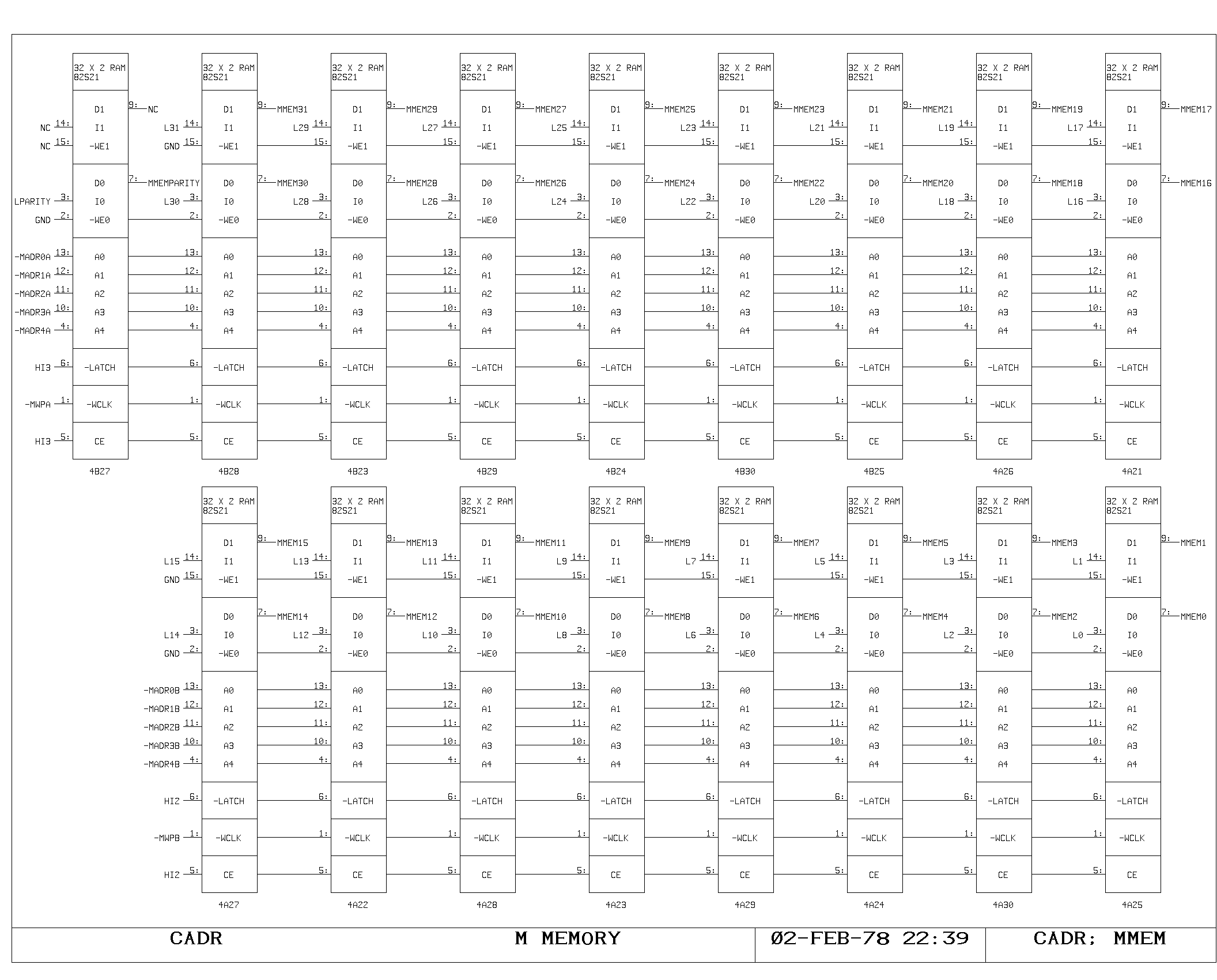
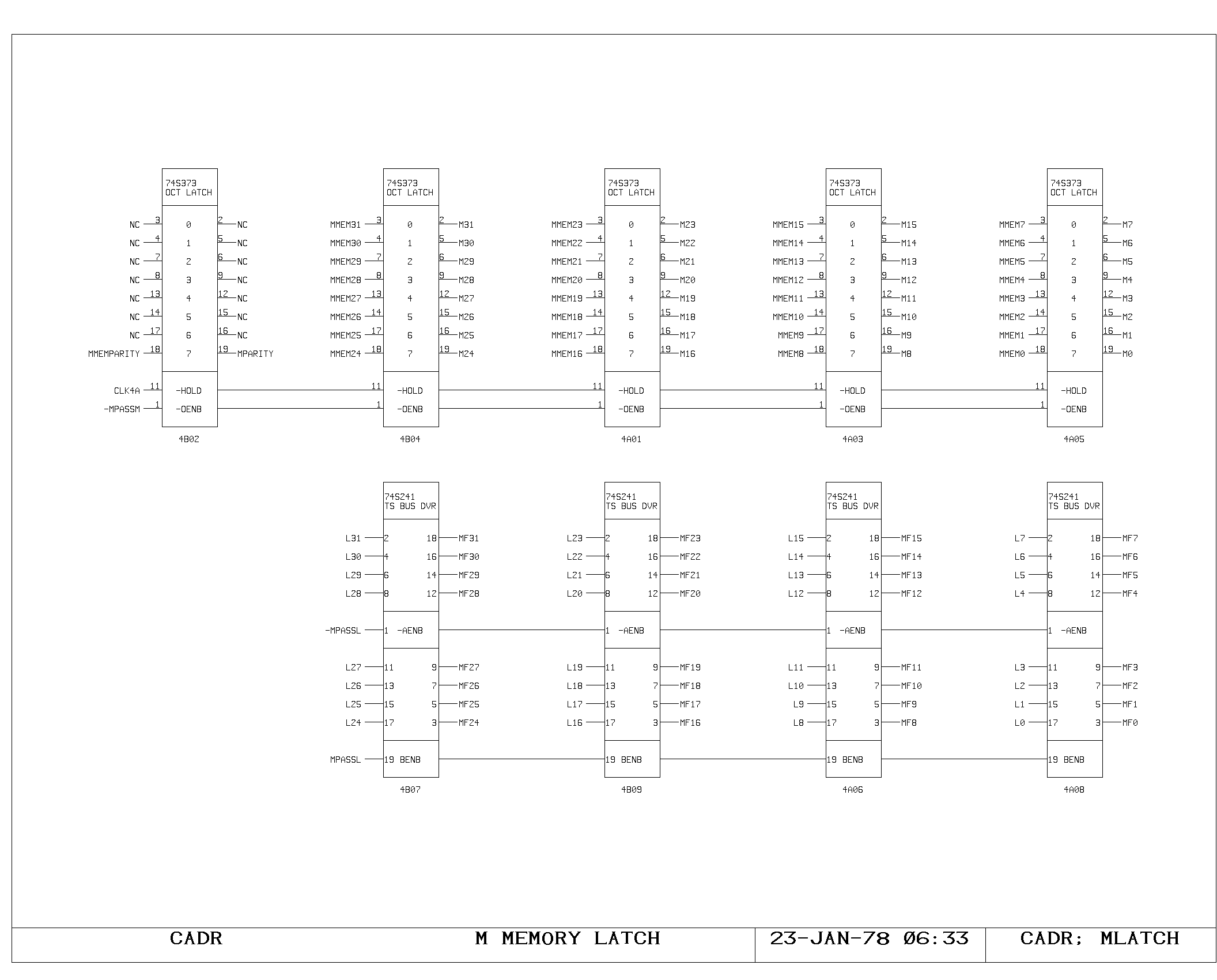
M Memory
Timing of M memory fetches and writes is very similar to timing of the
A memory, and is shown on the MCTL, MMEM, MLATCH prints.

The major difference is a two-level buffering of the M bus data,
introduced for loading reasons. The M bus is split into two parts: a
short bus, unbuffered for “slow” sources, and a long bus, buffered,
for “fast” sources. The short bus, labeled Mxx, is driven from the M
memory latches, the PDL buffer latches, the SPC latches, and from the
buffered outputs of the long bus. The long bus, labelled MFxx is
driven from all of the remaining M bus sources, including the L
register output, which is used for the pass around path. The MFxx to
Mxx buffers are shown on the MF print.

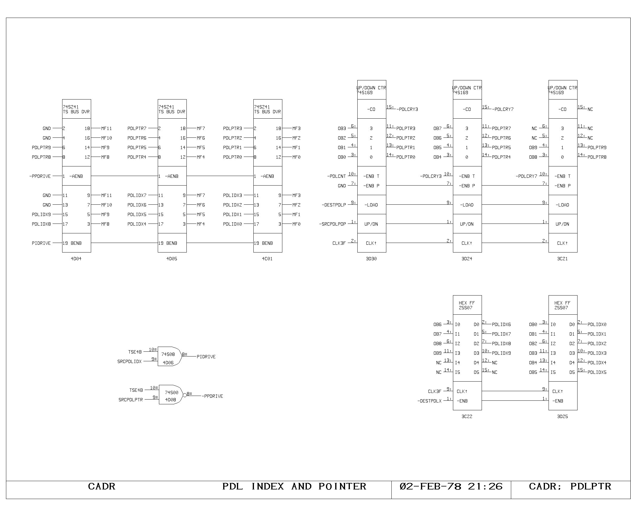
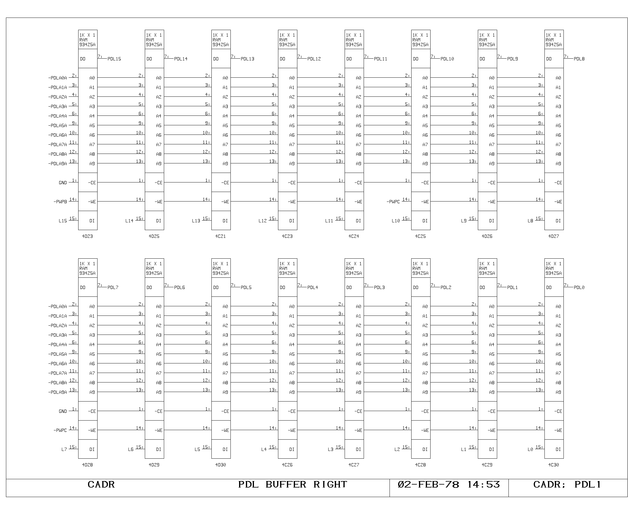
Stack Buffer
The stack buffer is addressed from one of two registers, the PDLPTR or
the PDLIDX. The PDLCTL print shows the address selector for the
buffer. During the first half of a cycle, the buffer performs a read
from either the address contained in the PDLPTR or the address
contained in the PDLIDX controlled by IR bit 30. The output of the
buffer memories (shown on PDL0 and PDL1) drive the inputs of the
latches shown on the PLATCH print. When the clock falls, this set of
latches holds the output of the buffer for the remainder of the cycle,
The latch output is driven onto the Mxx lines as an M source if the M
source field contains either SRCPDL or SRCPDLPOP.

The stack buffer address lines also change when the clock falls,
switching the address so that the results of the previous cycle’s
write in the stack buffer may be performed. If a write is to occur,
the PWPx write pulses are produced.

The PDLIDX and PDLPTR registers are conditionally loaded directly from
the output bus at the rising edge of the main clock. In addition, the
PDLPTR register can conditionally count up or down by one to perform
the push and pop operations. Due to the delay in performing the write
until the succeeding cycle, the post-decrement pop and pre-increment
push occur automatically due to the intervening rising clock
edge. Since pushing and immediately popping data on the stack is a
rather meaningless exercise, there is no facility in the stack buffer
for performing data passarounds. As a result, it is possible to
produce nominally correct, although inefficient, code which will
function incorrectly.

Either the PDLPTR or PDLIDX may be read onto the M bus as fast sources
buffered through the MF buffers.


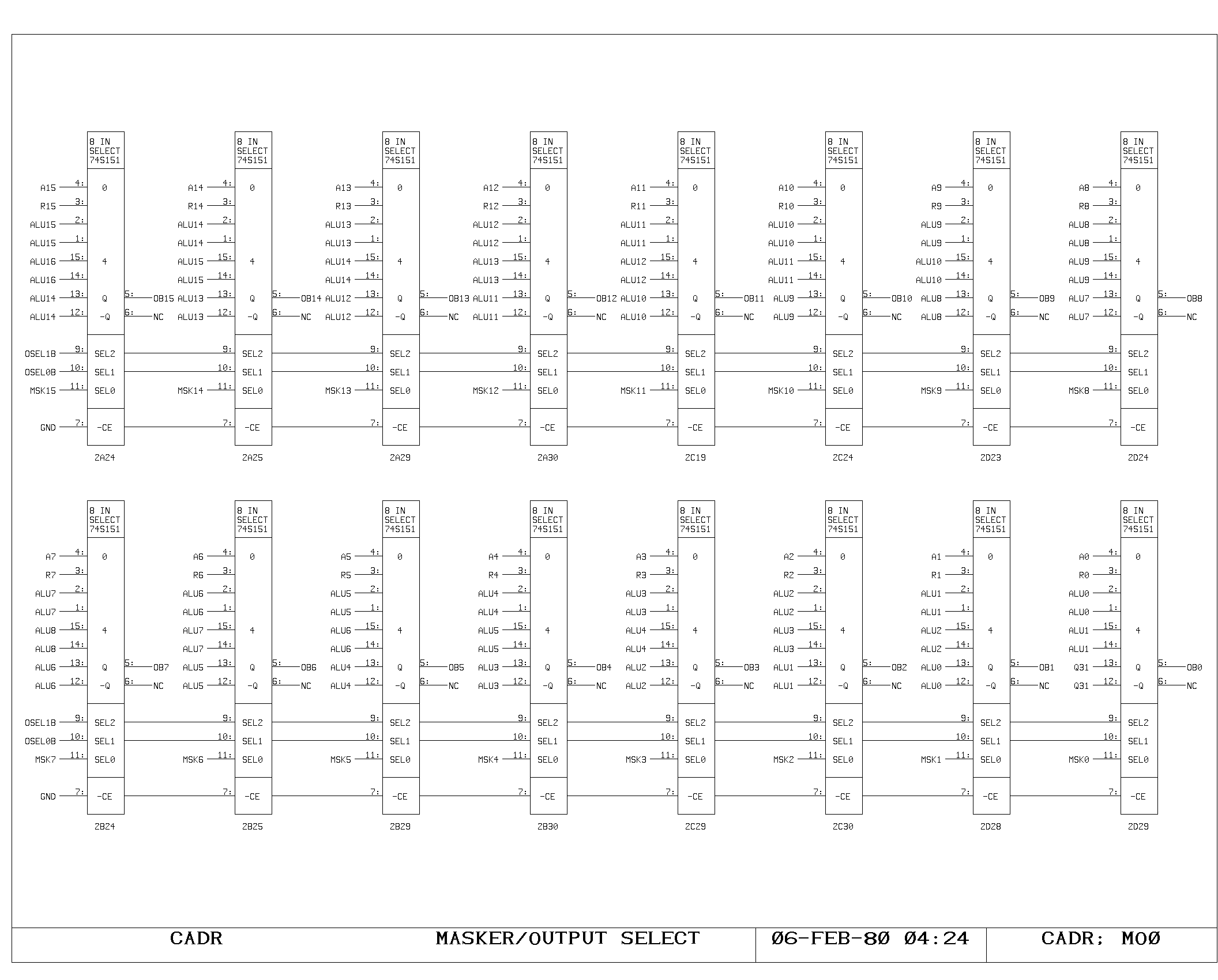
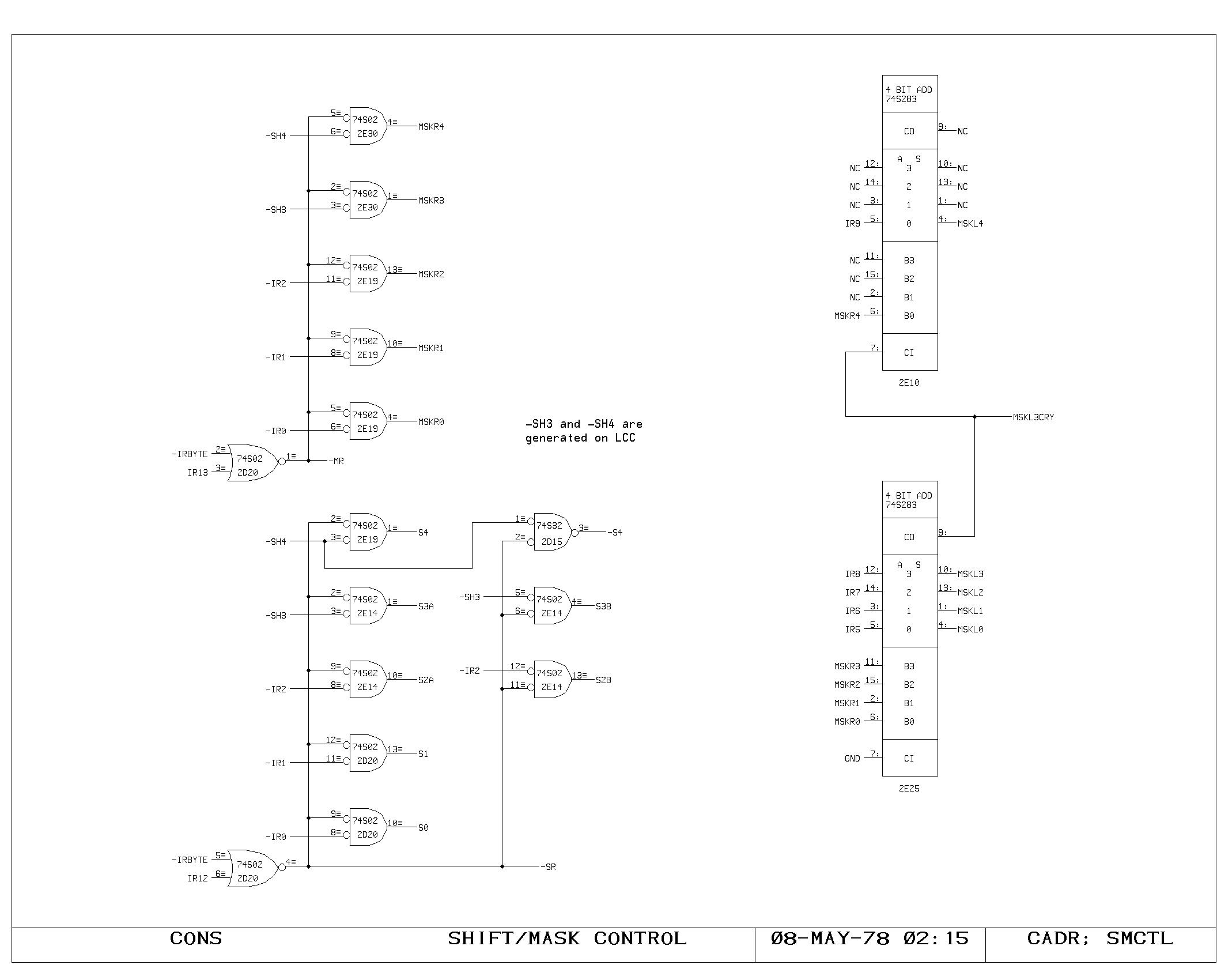
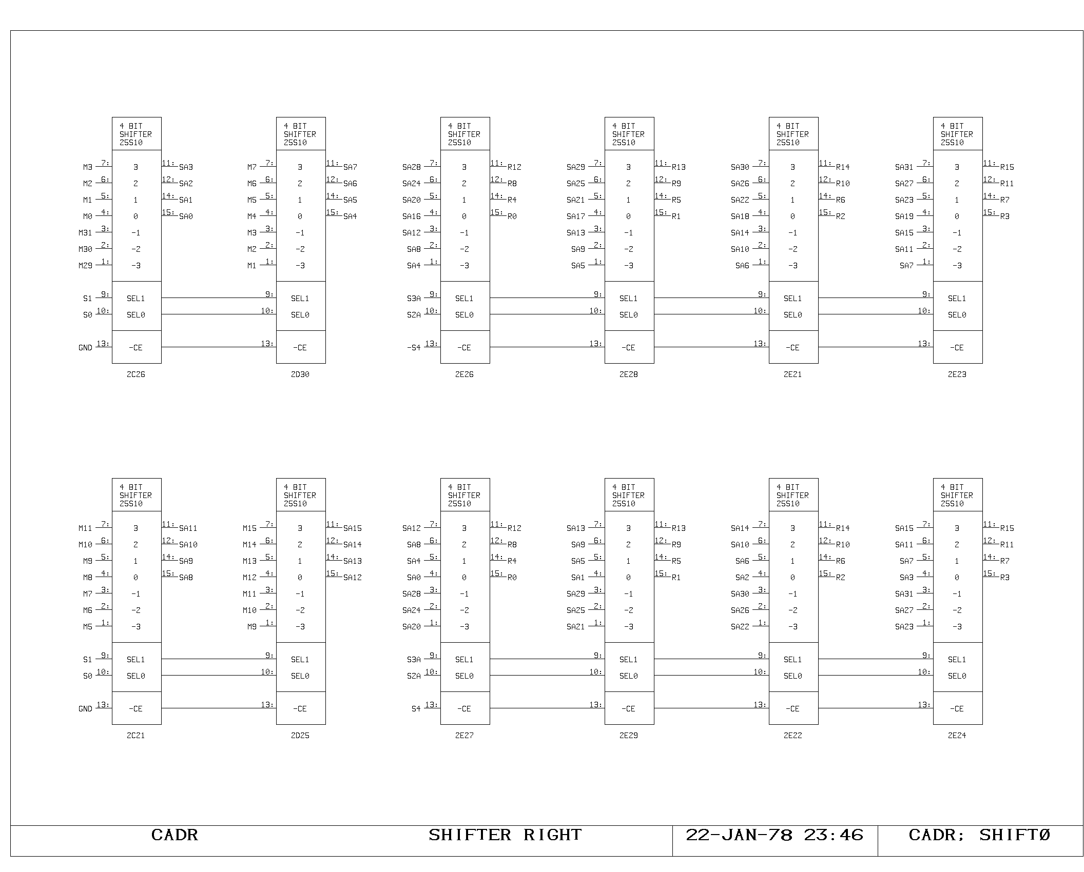
The Shifter/Masker
The A and M bus data drive both the ALU and the shifter/masker. The
shifter is controlled by a five bit shift field generated on the SMCTL
print. The shift is usually specified from IR4-IR0, but this selection
can be modified in two ways. In the selective deposit instruction, the
shift of the M source is forced zero, by setting IR bit 12 in a byte
instruction. In instructions referencing macroinstruction byte streams
of 8 or 16 bit words, the shift can be modified in bits 4 and 3 by the
contents of the macro program counter (LCC) if the miscellaneous
function 3 is selected (IR bits 10 and 11 on). This allows
instructions referencing a word containing this data to be
automatically shifted to examine the correct byte with no extra cycles
for performing shifts.
The specified five bit shift field is used to control a 32 x 32 shift
matrix set up as a rotator, as shown on the SHIFT0 and SHIFT1 prints.
The output of the shifter (Rxx) is used to drive both the masker and
the dispatch table address inputs,
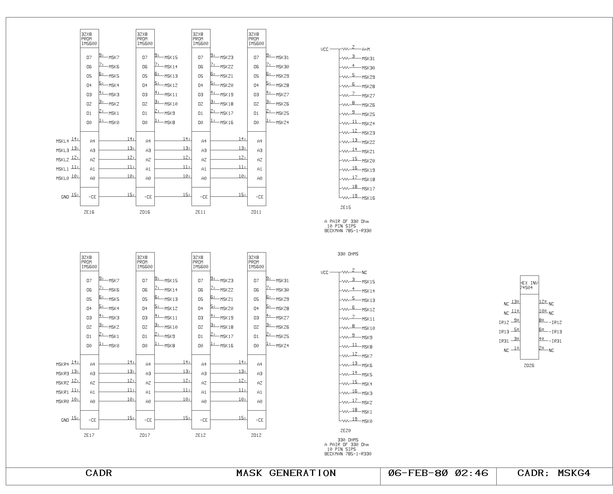
The masker performs a bitwise selection between the output of the
rotator and the A bus data. The selection is based on a third 32 bit
number, the mask (MSKxx). This number is produced from a set of two 32
x 32 programmable read only memories (print MSKGEN), whose contents
are OR'd. Each set contains a triangular bit pattern, working from
left to right in one set, and from right to left in the other.
The address inputs to these proms represent the left and right bit
positions of the selected field. The right bit position is either zero
or the same as the input to the shift matrix, as controlled by bit 13
in a byte instruction,
The left bit position is always produced by adding the contents of IR9
to IR5 to the right bit position. Thus, these IR bits control the
width of the masked field.
The actual masking operation requires both polarities of the mask, and
is performed with the non-inverting and/or gate as shown on the MASK
print. This is one of the more inefficient areas of the processor from
a package count standpoint, primarily because there is no package
efficient and fast device for implementing the bitwise select
operation.


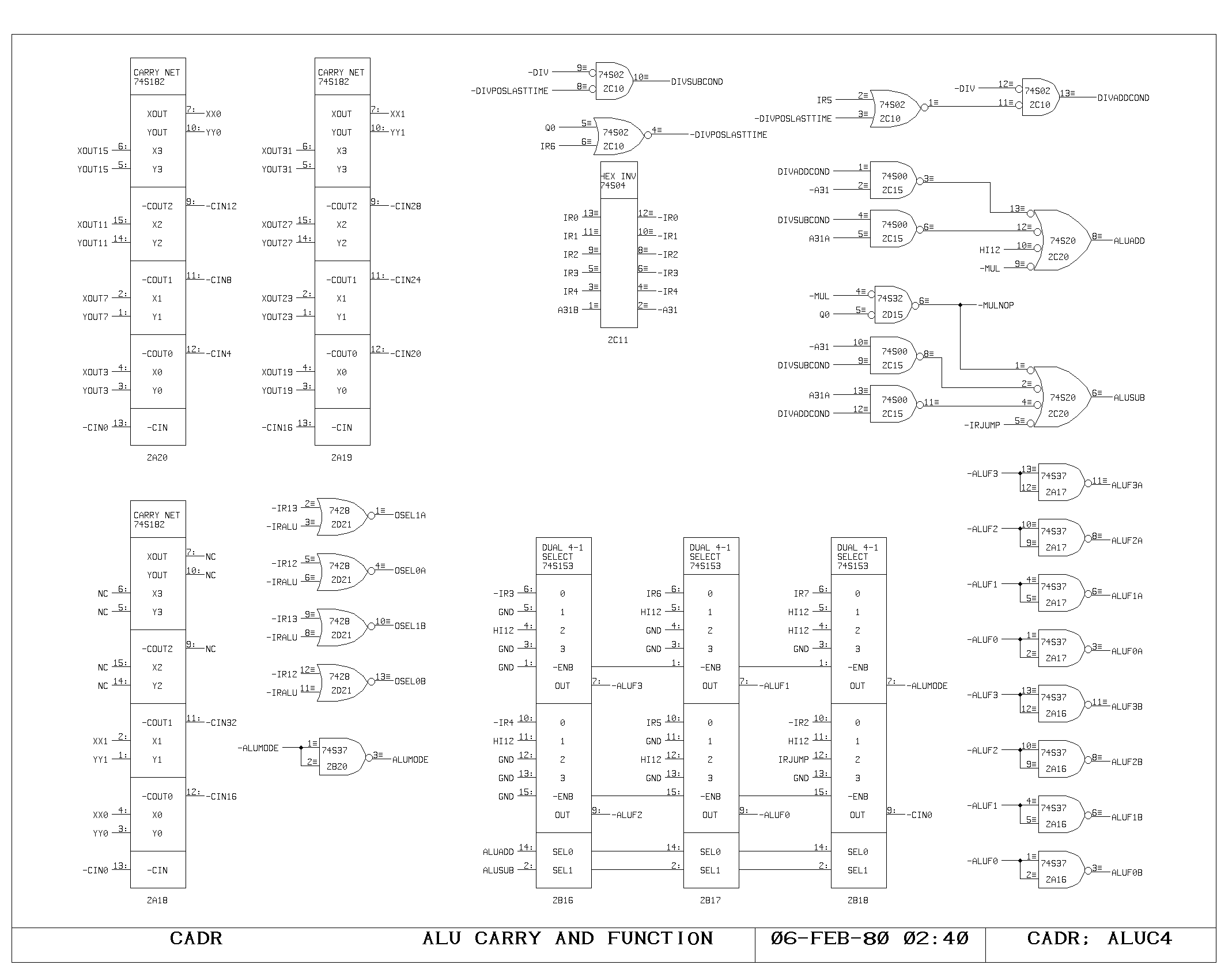
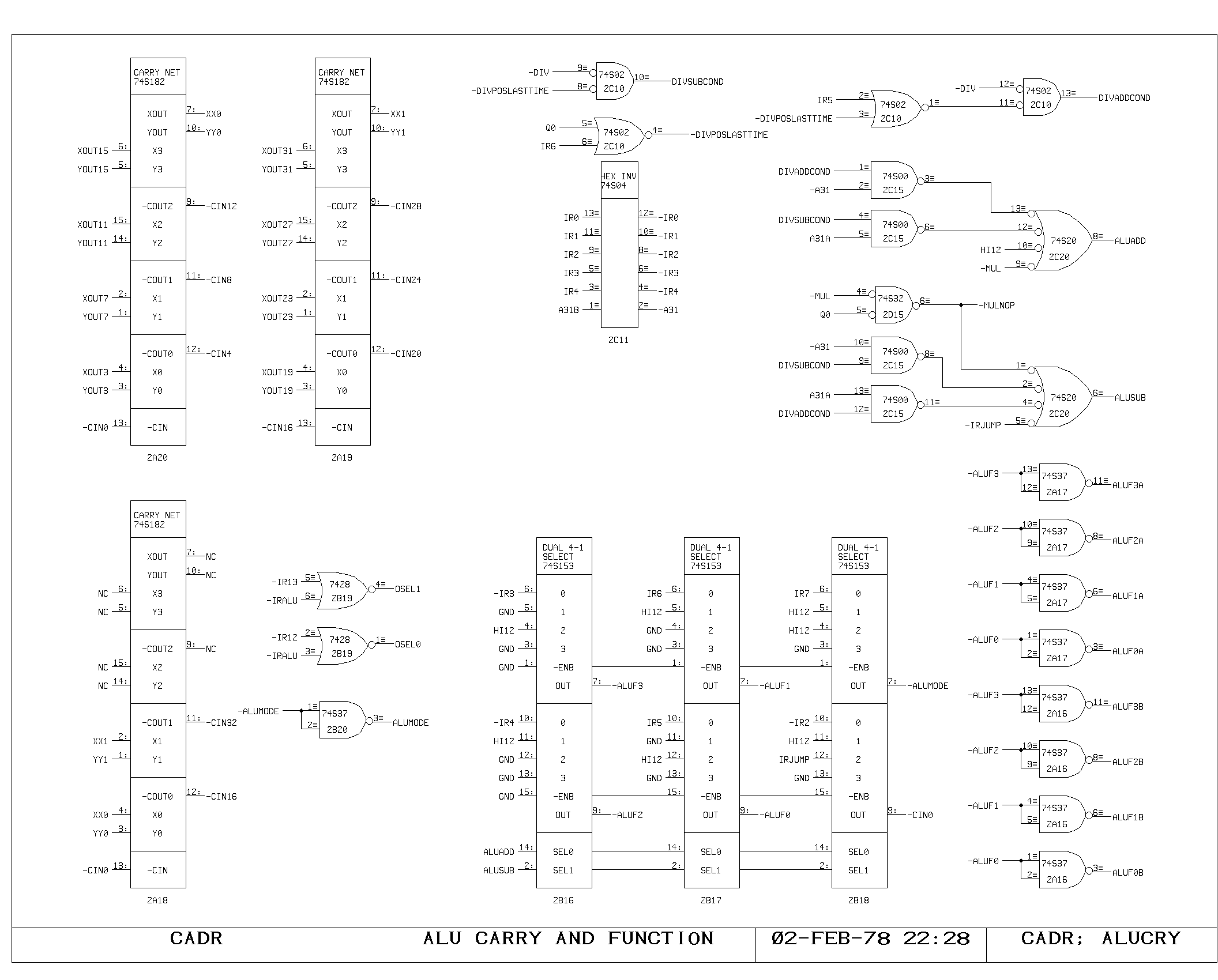
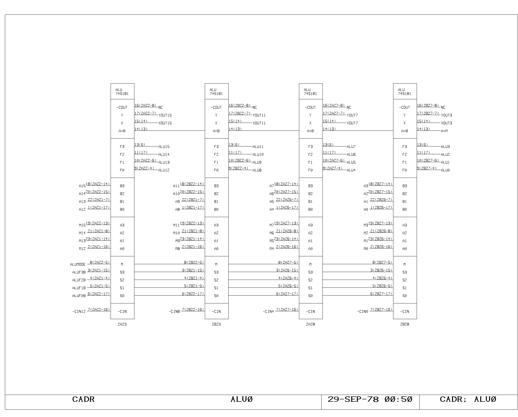
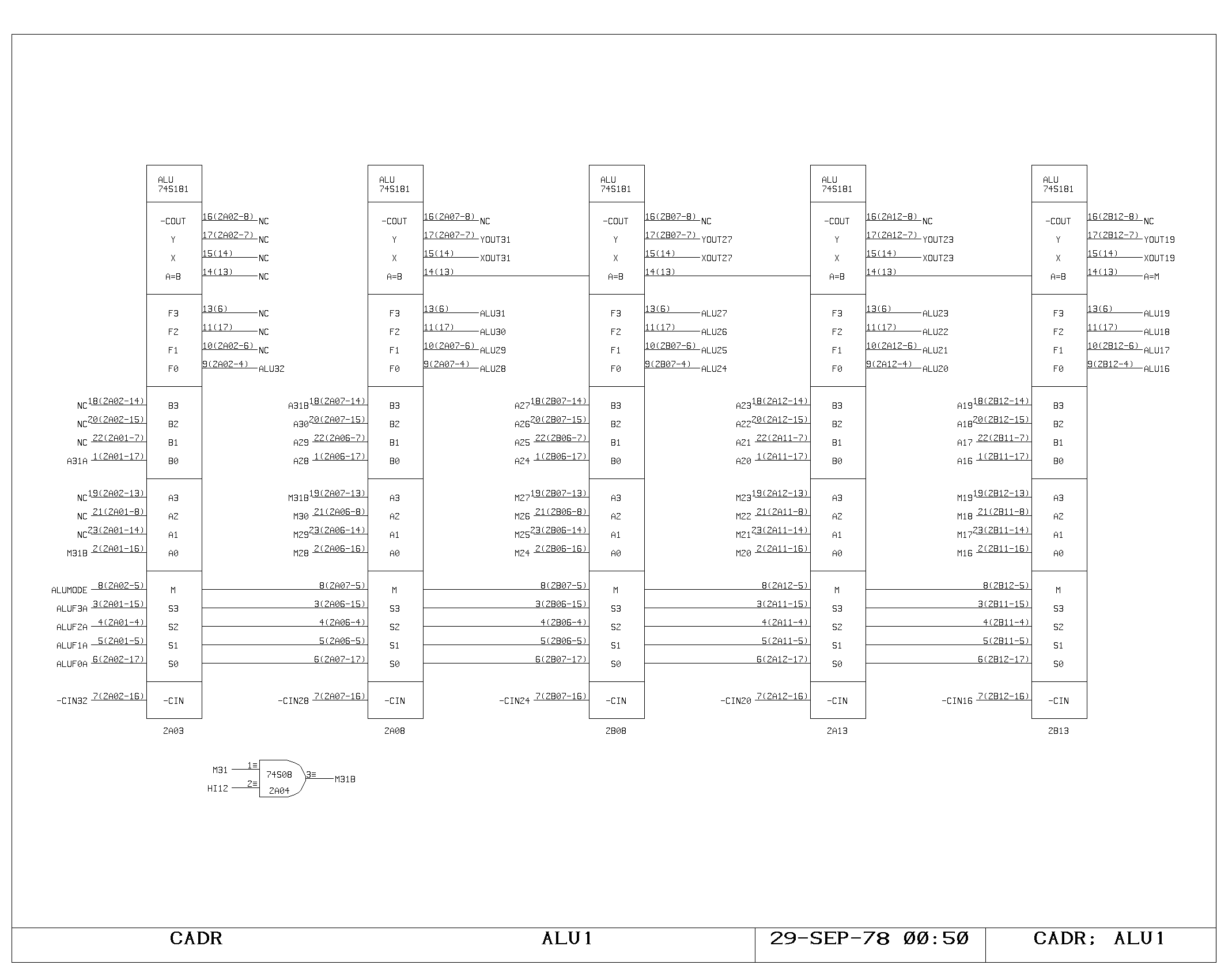
The ALU
The ALU performs the basic arithmetic in the machine. It consists of a
set of nine 4 bit arithmetic chips, with two levels of fast carry
extenders. The A and M busses drive the two inputs of the ALU
directly. The function performed by the ALU is controlled by the set
of selectors shown on the ALUCRY print. For the normal ALU
instruction, the function, mode, and carry inputs are controlled by
bits in the IR,

Three “hardwired” functions are also provided, by other selector
inputs. One is a hardwired add of the A and M bus data, invoked by
both multiply step and divide step under the appropriate circumstances
(controlled by the ALUADD signal). Another is the subtract operation,
invoked conditionally by the divide operation, and unconditionally by
all jump instructions (ALUSUB). The jump instruction subtracts the A
and M bus data, allowing an examination of the sign and equality
condition code outputs of the ALU. The third hardwired function simply
passes A memory data through, and is used as the NOP cycle during an
inactive multiply step (both ALUSUB and ALUADD asserted).
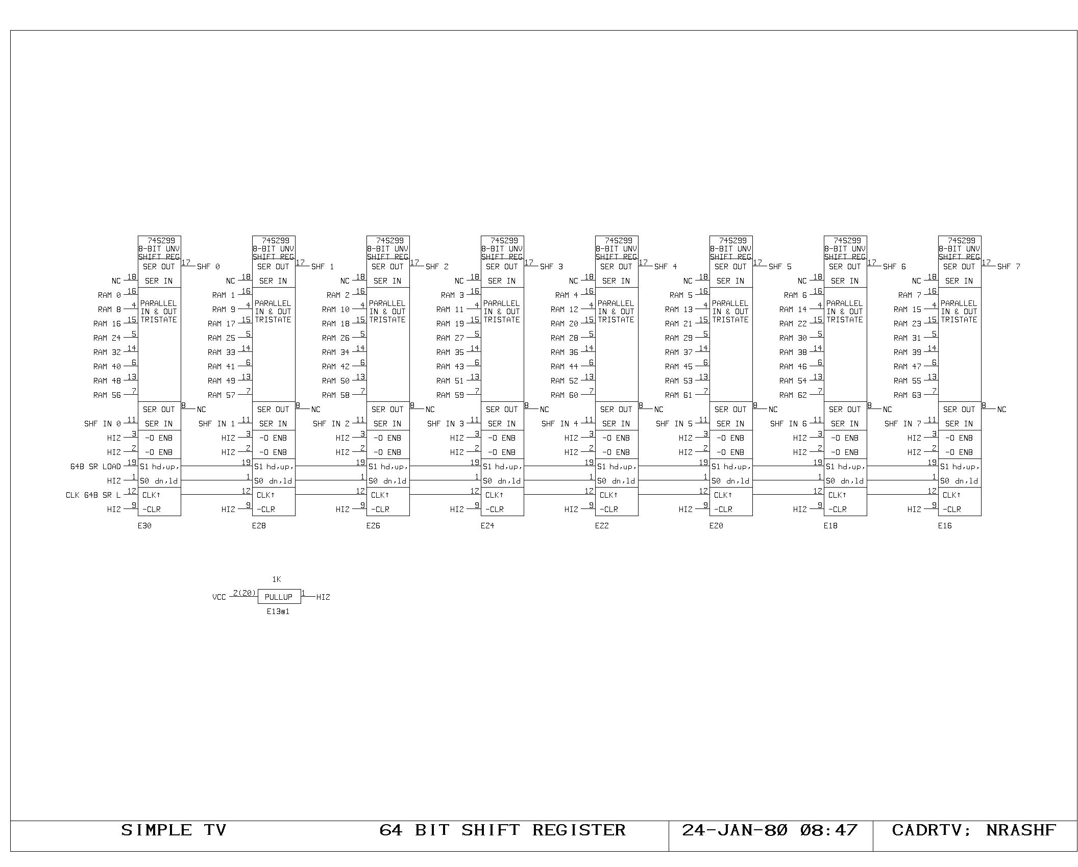
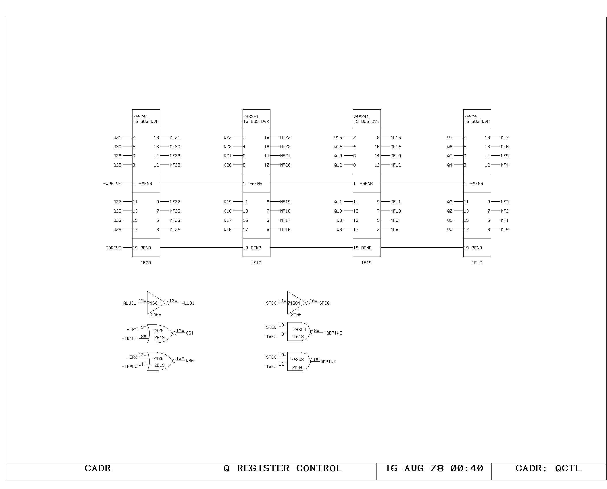
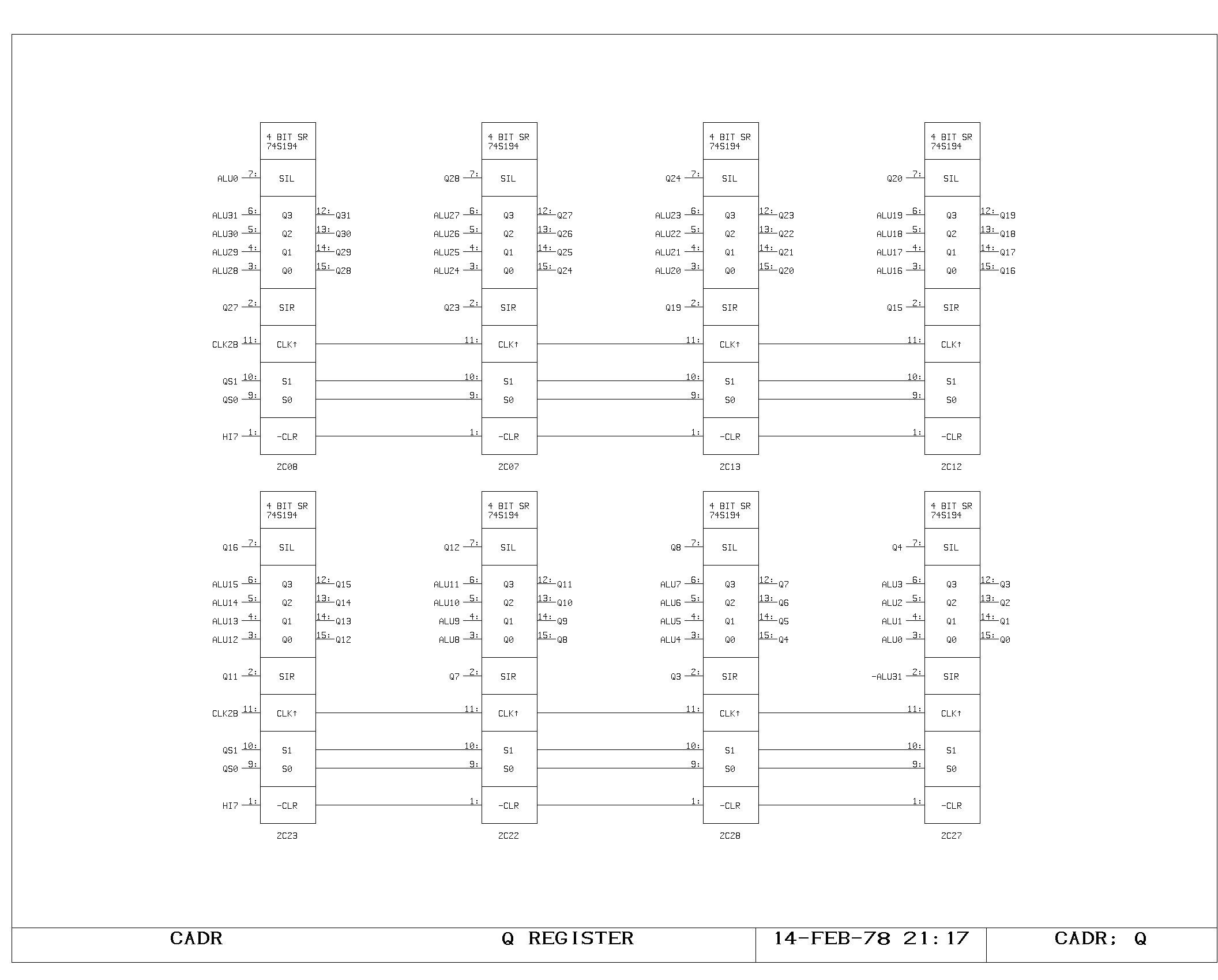
The Q Register
The Q register forms the remainder of the multiply-step and
divide-step hardware. It stores low order product bits as they are
produced by the multiply step, and is used to store both dividend and
quotient bits during a divide step operation. It consists of a 32 bit
shift register which can be loaded from the ALU output, shifted left,
or shifted right. It is controlled by IR1 and IR0 in an ALU
instruction (QCTL). It acts as a fast source on the M bus, and is
altered on the rising edge of the main clock.

Shifts in from the left are from the low order bit of the ALU (useful
for the multiply step), while shifts in from the right are from the
complement of the sign of the ALU output, which is the correct data
for the partial quotient in a divide step.
The Output Bus
The primary result of either BYTE or ALU instructions is placed on the
output bus (OBx). The output bus is heavily loaded, and drives all of
the processor registers, except the Q, which are clocked on the rising
edge of the main clock. During BYTE instructions, the output bus
selector is forced to pass data from the masker (ALUCRY
print). Otherwise, the selector is controlled by bits 12 and 13 in an
ALU instruction. The selector may select either the unshifted ALU
output, which is the normal case, or the ALU output shifted left by
one, with the low bit coming from the high order bit of the Q, or the
ALU output shifted right by one, with the high order bit coming from
the one bit ALU extension,

The output bus bit shifting paths are again chosen to make the
multiply step and divide step operations occur in a single cycle.

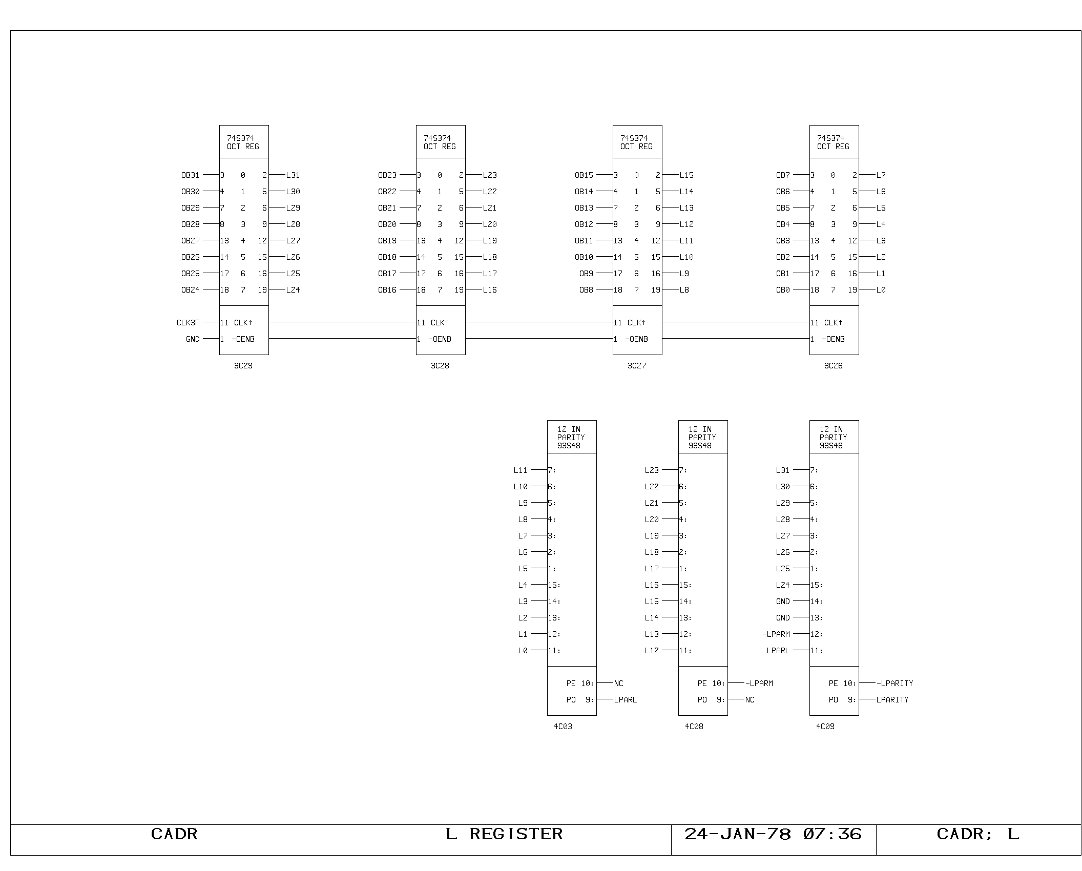
The L Register
The L register provides a clocked version of the output bus data from
the previous cycle. It is used as the source of write data for all of
the memories which are written with write pulses in the second half of
the succeeding cycle, and as a source of operand data on the A or M
bus when the passaround logic is activated by sequential write-read
instructions to the same memory location.
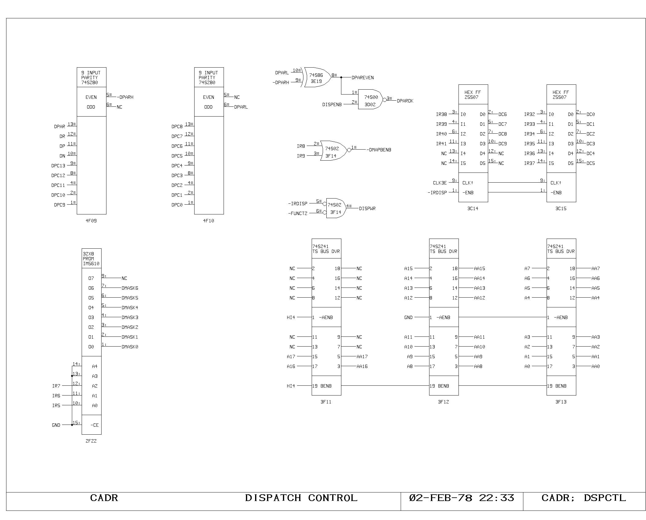
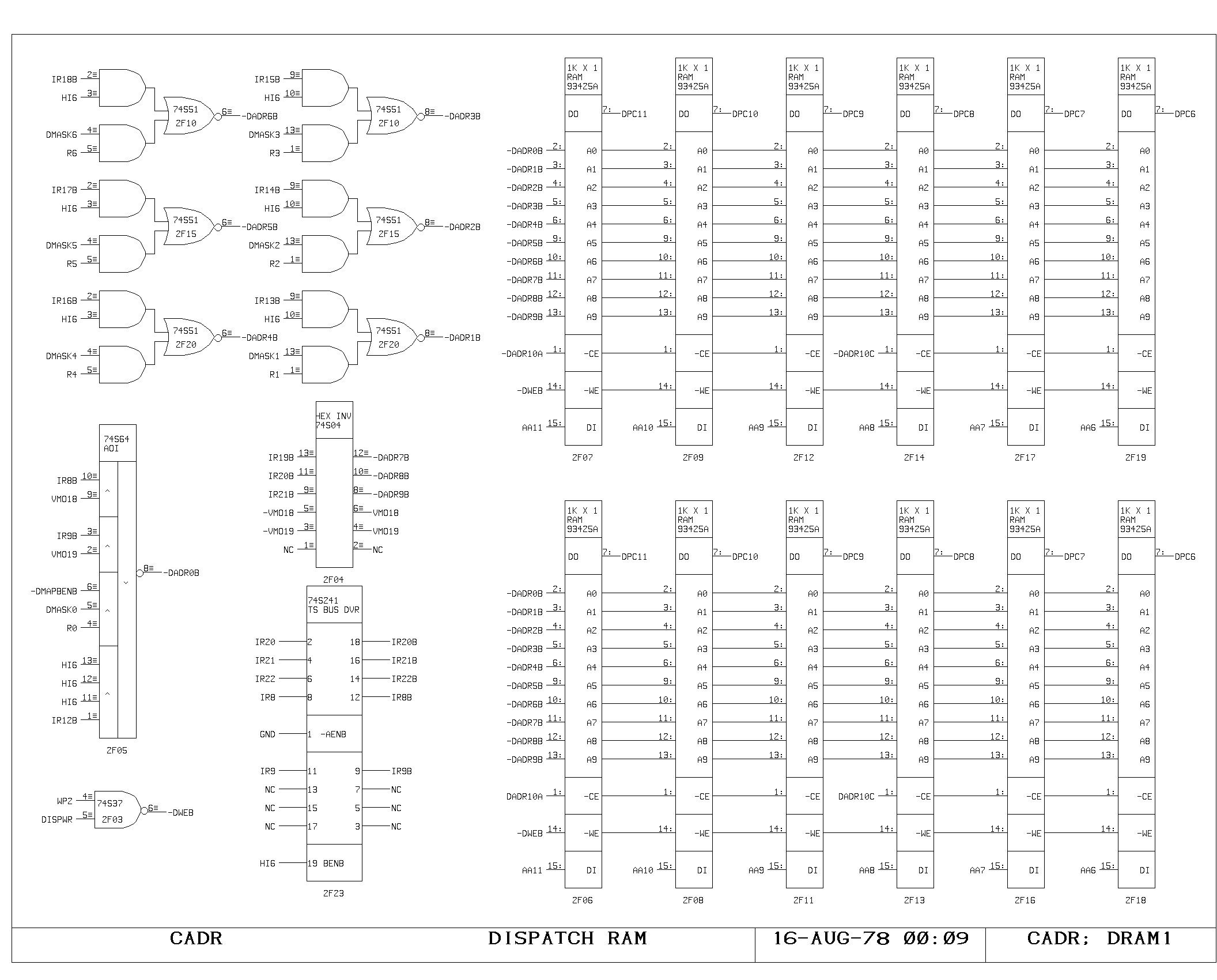
The Dispatch Memory
The dispatch memory is used to produce new program counter values as a
result of data flowing through the processor. Qutputs of the shifter
(Rxx) are AND'd with a dispatch byte length mask, and OR'd with an
eleven bit field from the IR to form the dispatch memory address,
DADRxx (left hand side of DRAM0,1,2). Bit zero of ihe dispatch address
additionally may be taken from the output of the memory map (see
below). The mask used for selecting the dispatch byte length is
located on the DSPCTL print, as are the buffers for A bus data which
is used for writing into dispatch memory. The dispatch memory, unlike
all other memories in the machine, is loaded in the same instruction
which specifies the write, since its output is needed late in the
cycle and cannot be latched as can the other processor memory outputs.

Output of the dispatch memory is a new 14 bit program counter value
and three additional bits, DN, DP, and DR, which control the type of
transfer performed (see control discussion below).


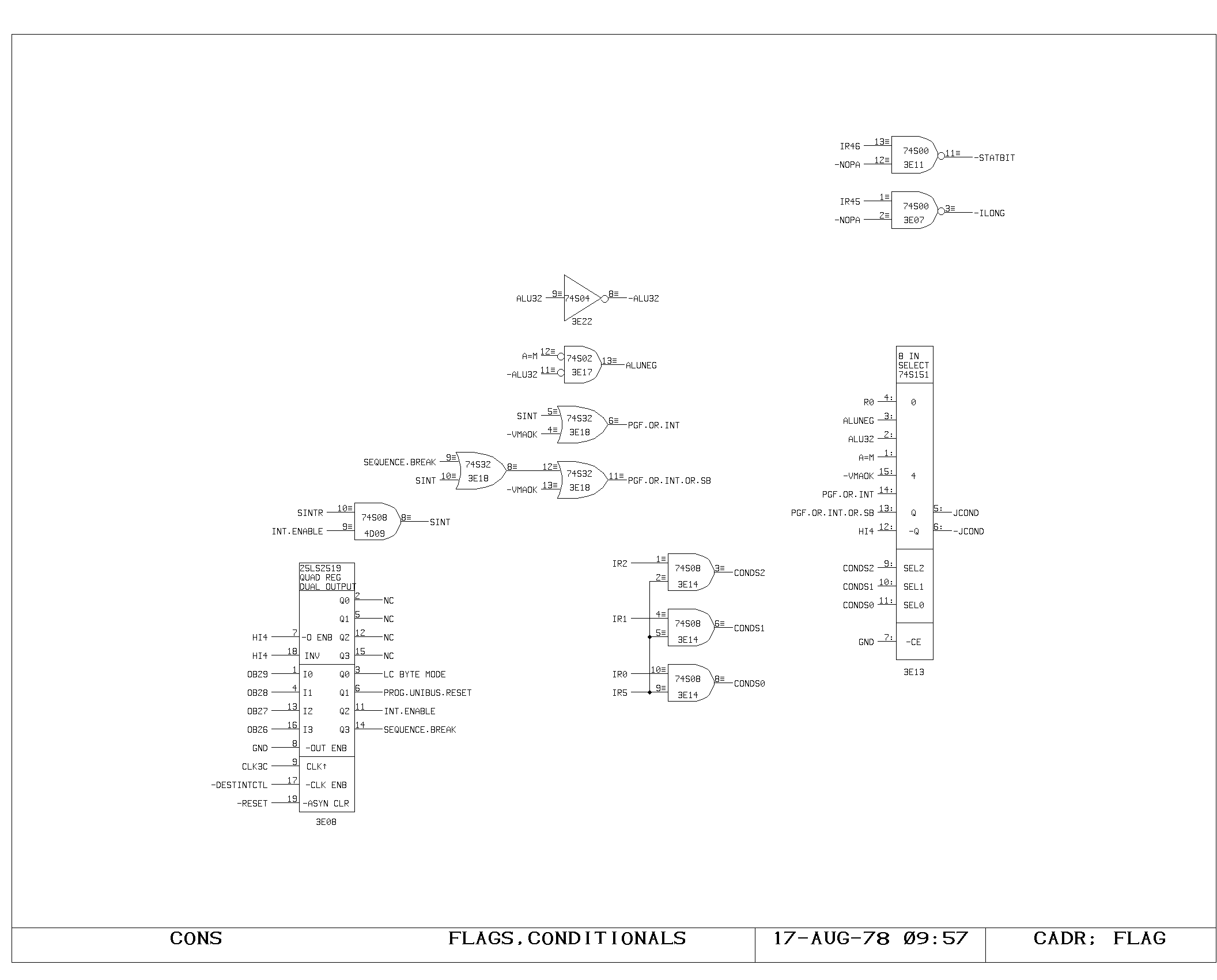
Jump Conditions
The FLAG print shows the jump condition selector, which is used to
determine what controls the success of a conditional jump. If IR bit 5
is zero, the low bit of the rotator output (R0) is selected, and the
field IR4-0 is used for controlling the rotator. Otherwise, bits 2-0
control the jump selector, which examines the ALU sign and equal zero
outputs in various combinations to provide arithmetic compares. The
selector also has access to the page fault condition (-VMAOK) and
combinations of it with interrupt and sequence break conditions, so
that these combinations may be easily tested in a single cycle.
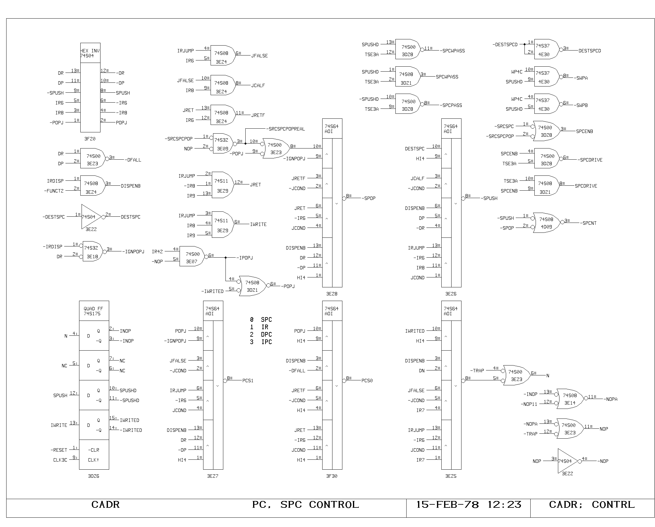
Flow of Control
The CONTRL print implements the different types of jump and dispatch
transfers. Three sources influence the transfer of control: the jump
instruction data, the dispatch instruction data, and the
POPJ-AFTER-NEXT bit.

The jump instruction is further decoded into special cases prior to
the availability of the condition output. For the PC source, the jump
selects between IPC (no jump), IR (jump or call) and SPC data
(return). If the transfer is taken, the value of IR7 is selected for
N, which controls execution of the following instruction.

The dispatch instruction similarly specifies with DP and DR, the PC
source and N outputs, selecting the new PC from DPCxx (output of the
dispatch memory), IPC (fall through) or SPC (return). The N bit is
driven directly from the DN output of the dispatch memory,
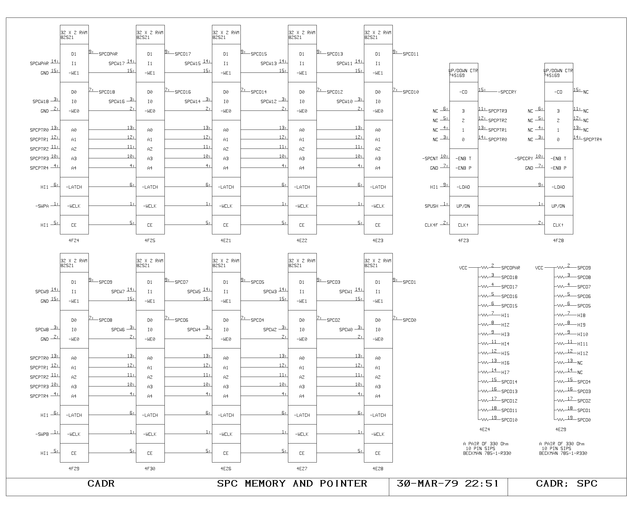
Microcode Subroutine Return Stack
The return address for micro subroutine calls is kept in the 32 entry
SPC memory. This memory is addressed by a five bit counter, the
SPCPTR. On micro subroutine calls, this counter is advanced, and the
subroutine return address is written into the memory. This address may
be one of four quantities, the current PC, the incremented PC, the
previous PC, or the L register contents.

The decision as to which PC to write on a call is based on whether the
call specified execution of the following instruction (PC or IPC) and
on whether it is an error catching dispatch, with the intention of
allowing retry (LPC). Writing into the memory from the L register
allows normal restoration of processor state information, as well as
allowing the machine to set the special flags in the left half of the
SPC register. One of these flags activates the macroinstruction
prefetch mechanism when a return is executed with that bit set.

The data contained in the SPC memory is read in two independent paths,
one driving the M bus, and the other driving the inputs to the next PC
selector (NPC). This allows the stack data to be read from the main
data paths, and to be used as a return address in jump and dispatch
instructions. Pass around paths are provided on the SPC output path to
the NPC selector, but are missing on the M memory path, since the data
is available from other registers in the machine after an SPC write
cycle.
Next PC Selector
The NPC selector determines the location of the next microinstruction
fetch.  It loads one of four potential sources for the next program
counter into the PC register, whose contents directly drive the
microinstruction memory addresses. The four sources are the output of
the SPC stack (SPC), the instruction register (IR), the dispatch
memory outputs (DPC) and the incremented PC (IPC). The PC may also be
forced to a zero by the TRAP signal, used for initial bootstrap, and
main memory parity errors. The output of the NPC selector is loaded on
each clock into the PC register, and the incremented PC is developed
with an adder chain from the PC register.

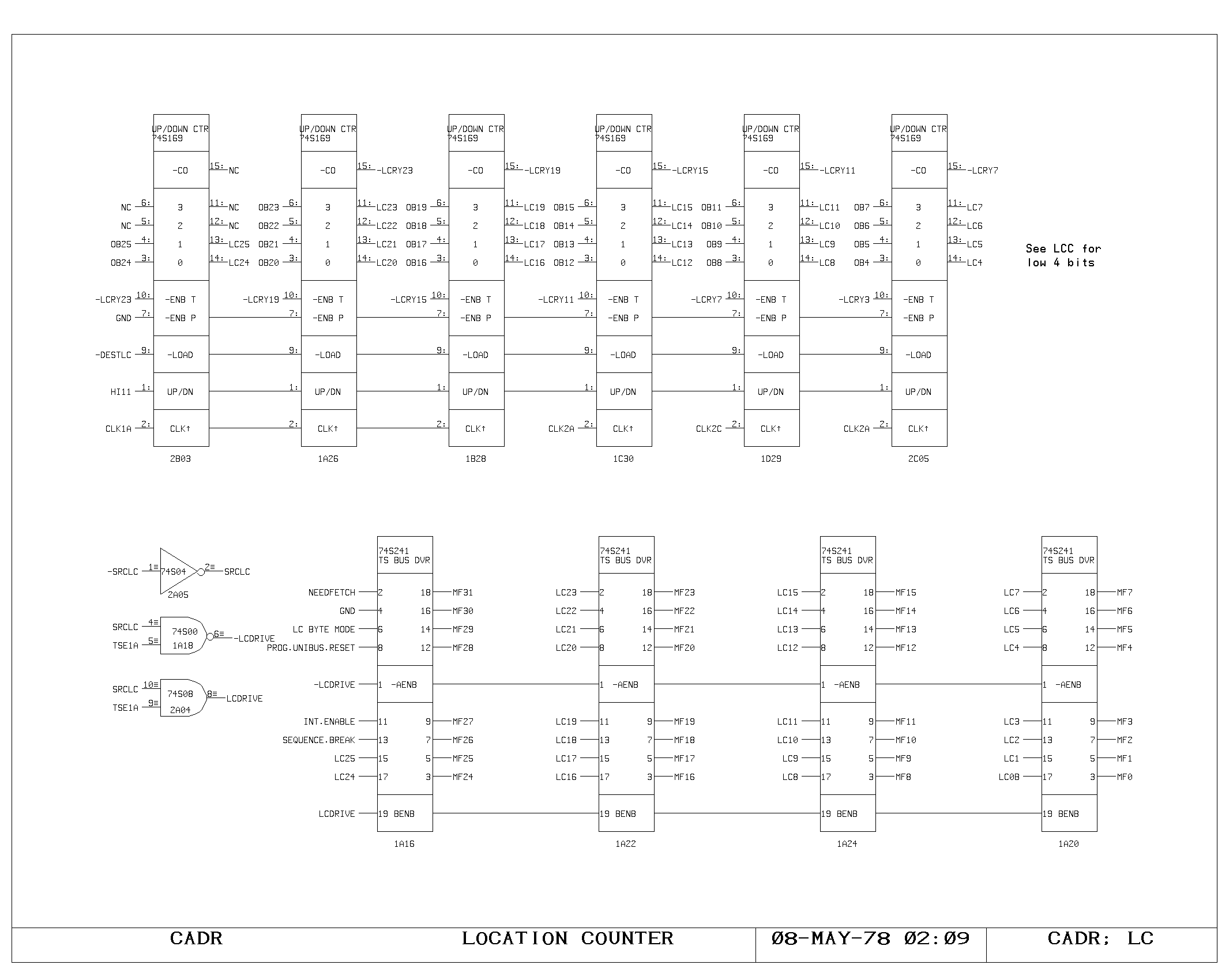
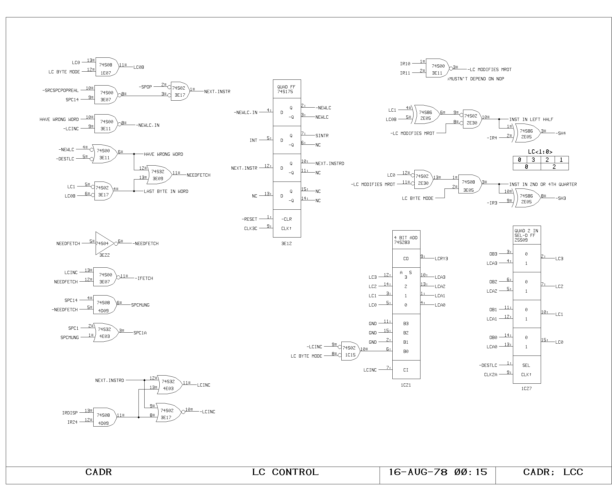
The LC register and Instruction Prefetch
The LC register provides an efficient mechanism for executing 16 bit
and 8 bit macro instruction streams with the processor. LC contains
the byte address of the next macroinstruction to be executed. When the
SPC return memory flag specifying the end of a macroinstruction
execution is set, the contents of LC are incremented by one or two
(depending on the 8/16 bit instruction flag). Then, if the last byte
of the macro instruction was just used, a main memory fetch is
initiated, loading the memory address register from the LC register,
shifted right by two.

During the course of macroinstruction execution, the LC register
contents influence execution of all microinstructions with the
miscellaneous field set to three. This specifies that the shift and
mask select for the current operation is operating on a macro
instruction word, and the value of the shift field is to be modified
according to the low order bits of the LC, resulting in the selection
of the proper half or quarter of the macro instruction word as data in
the modified microinstruction.
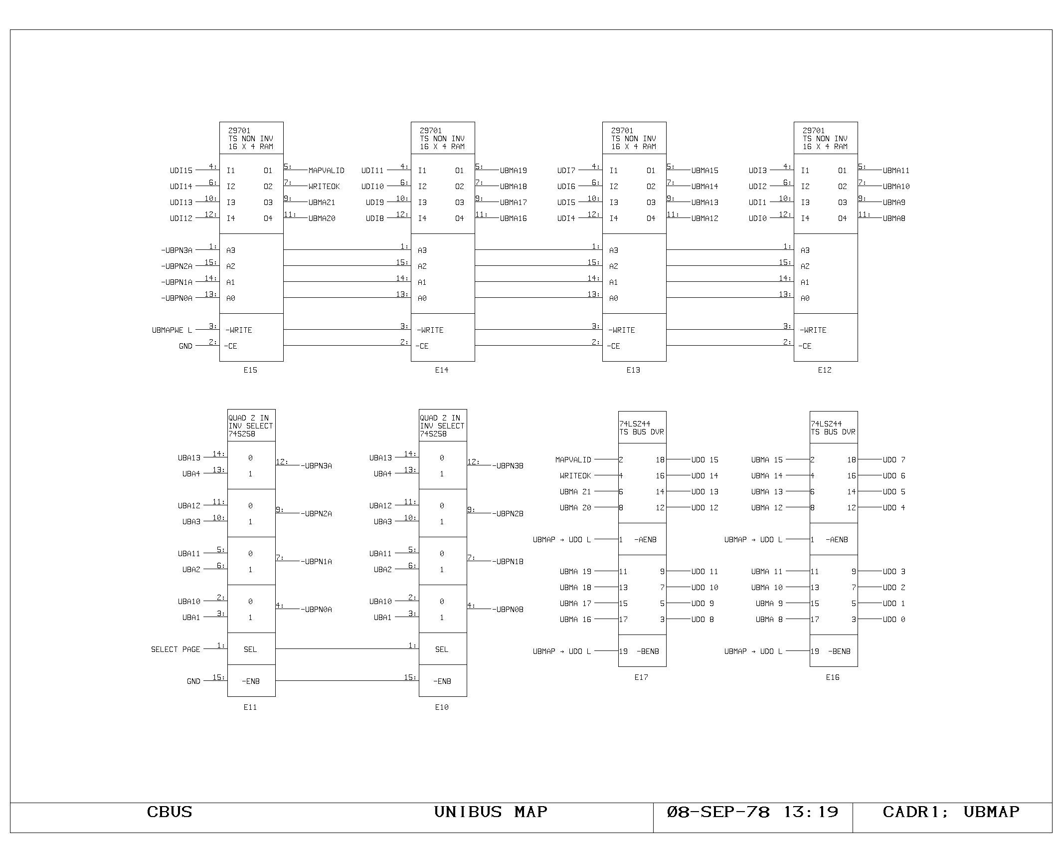
The VMA and VMA Selector
The VMA is a 32 bit register which holds the virtual memory address
being fetched by the processor. It is normally loaded from the output
bus, but may also be loaded during the macroinstruction prefetch
sequence from the (shifted) LC register contents. The output of the
VMA may drive the MF bus for access from the main data paths.

During one cycle prior to the initiation of a main memory cycle, the
output of the VMA drives the virtual memory map inputs though the MAPI
selector. This takes bits 23 though 8 (the virtual page number) and
maps them into a physical page number. Bits 7 through 0 are passed
directly to the memory system as an offset within the page.


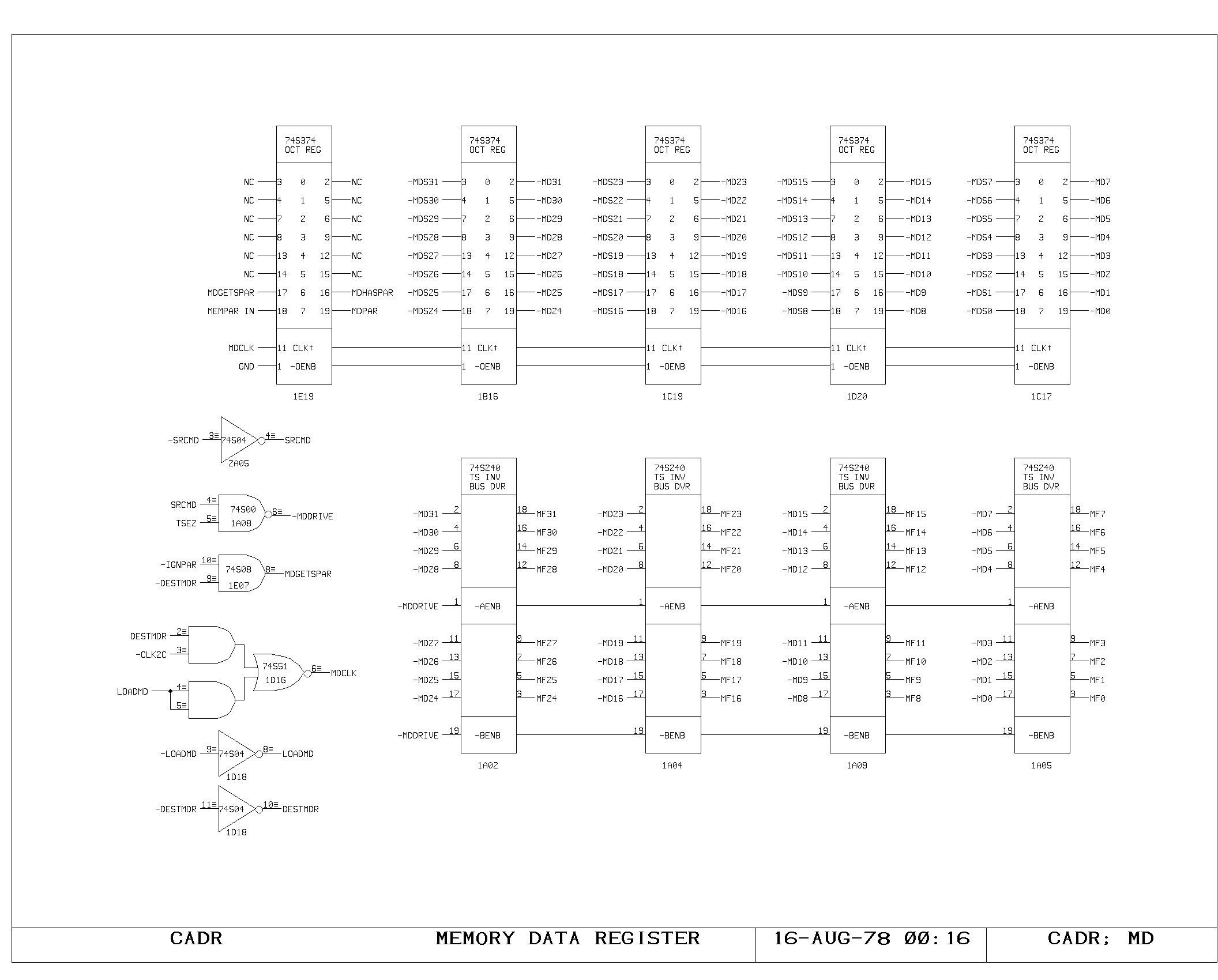
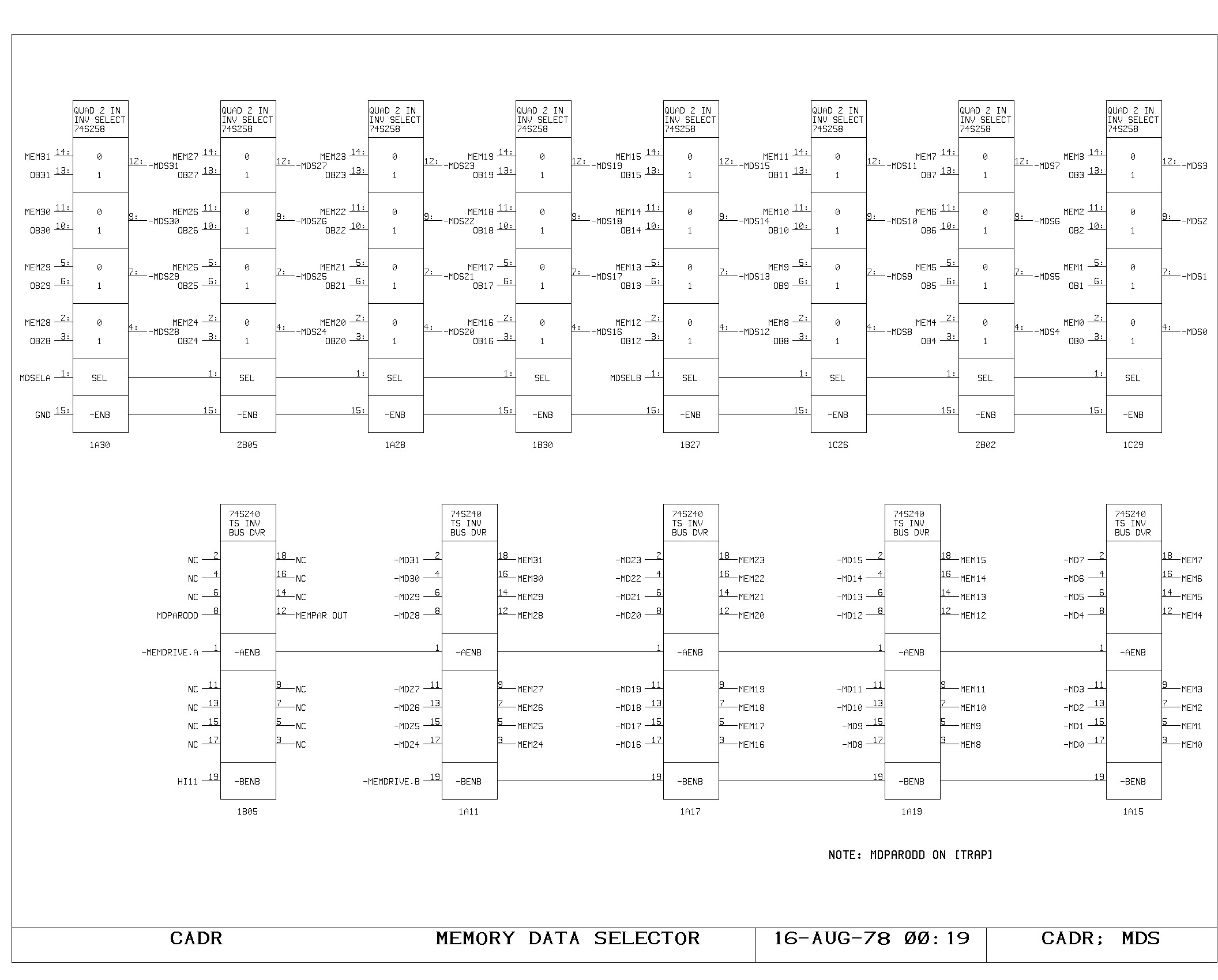
The MD and the MD Selector
The MD is a 32 bit register holding the contents of a main memory word
which is being read or written. Data is loaded into the MD from either
the main memory system (through the MEM bus) or from the output
bus. Output of the MD register drives the MEM bus (for memory writes),
the MF bus for access from the main processor data paths, and the
virtual page map input selector.

Access to the virtual memory map is provided so that the operation of
checking the data type and newspace/oldspace pointer location can be
effectively done simultaneously.  Normally the map input selector is
driven from the MD register, allowing newly fetched data coming into
the MD to be looked up in the map and drive the main data paths for
the dispatch instruction on the data type simultaneously.
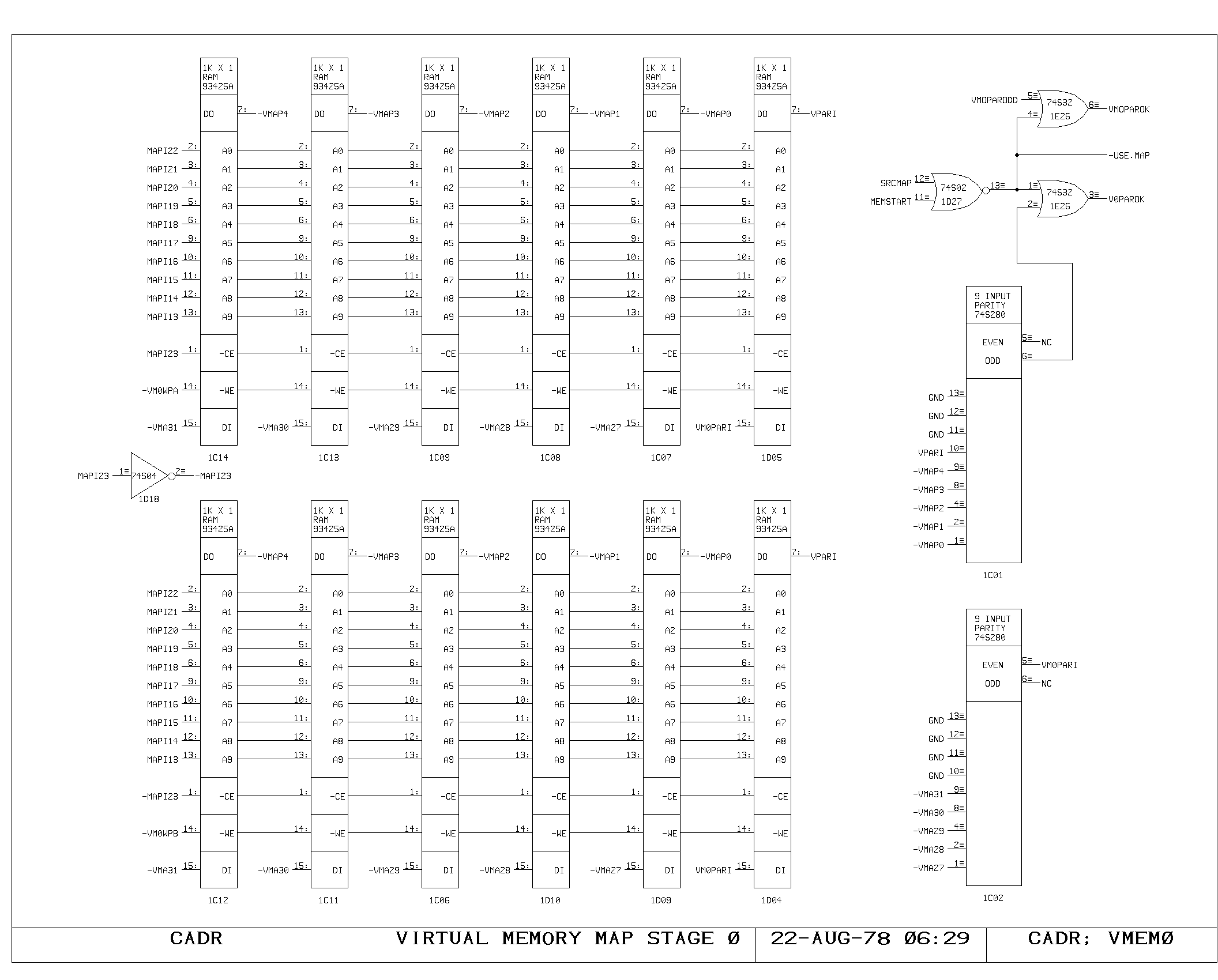
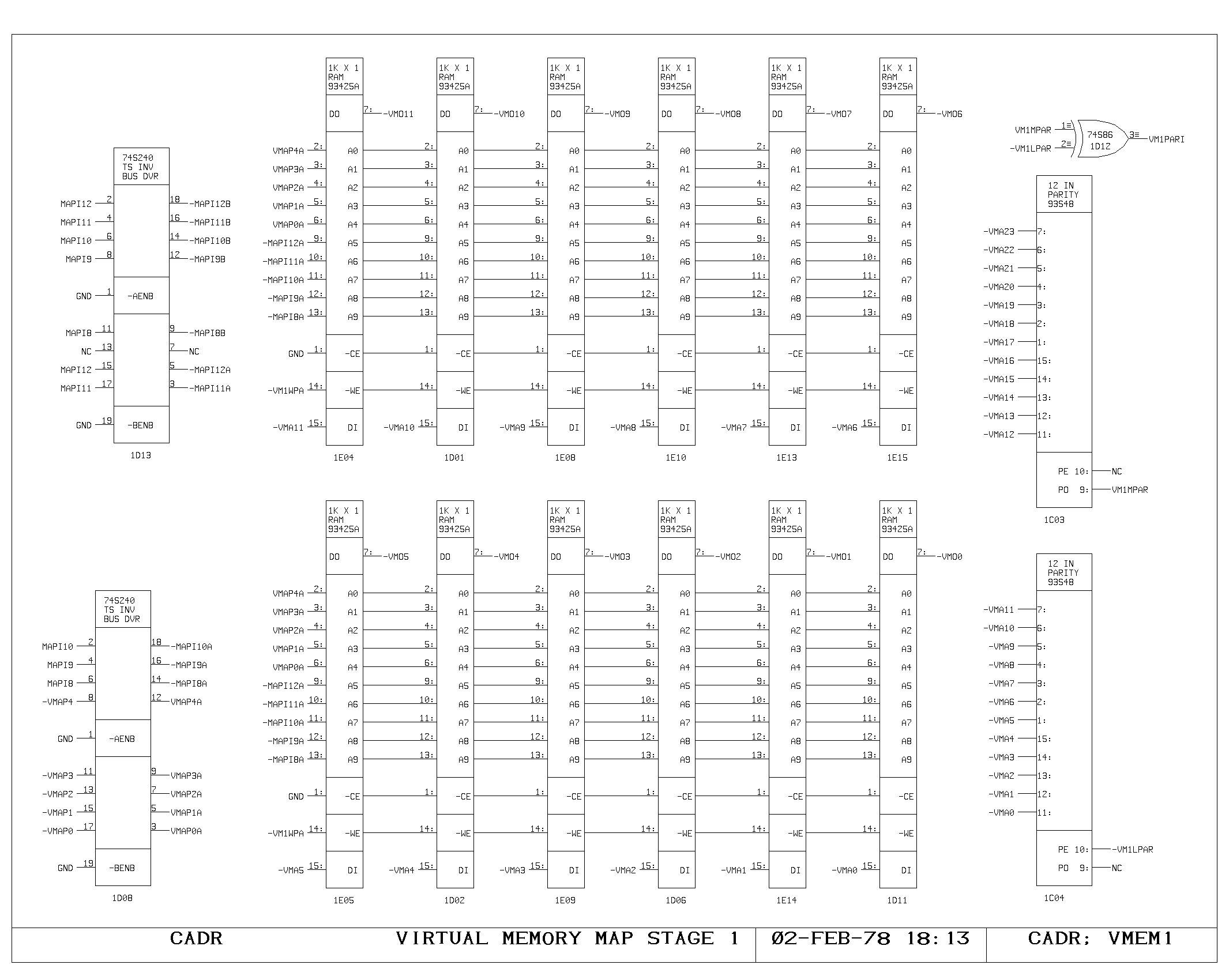
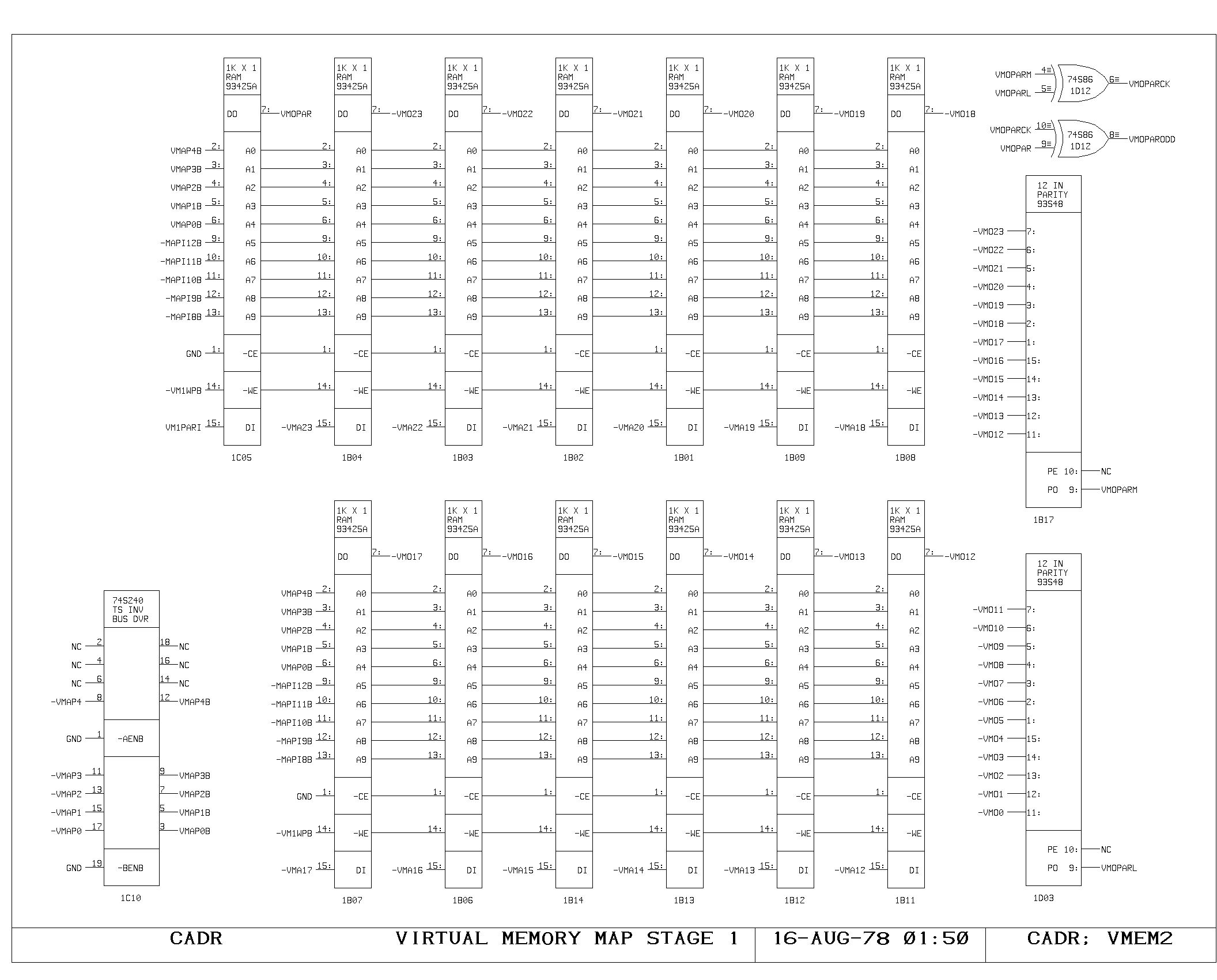
First and Second Level Maps
The virtual memory map is implemented as a two level table lookup
map. The map input selector drives either the MD or VMA contents onto
the MAPI lines. Bits 23 through 13 address a 2K by 5 memory, the first
level map on the VMEM0 print. Of the possible 2048 entries in this
table, a maximum of 31 are non-zero, producing non-zero outputs on the
five VMAP lines. The five VMAP signals combine with the map input bits
12 to 8 to address the second level map, on prints VMEM1 and
VMEM2. The second level map is a 1K by 24 bit memory, holding map
entries.
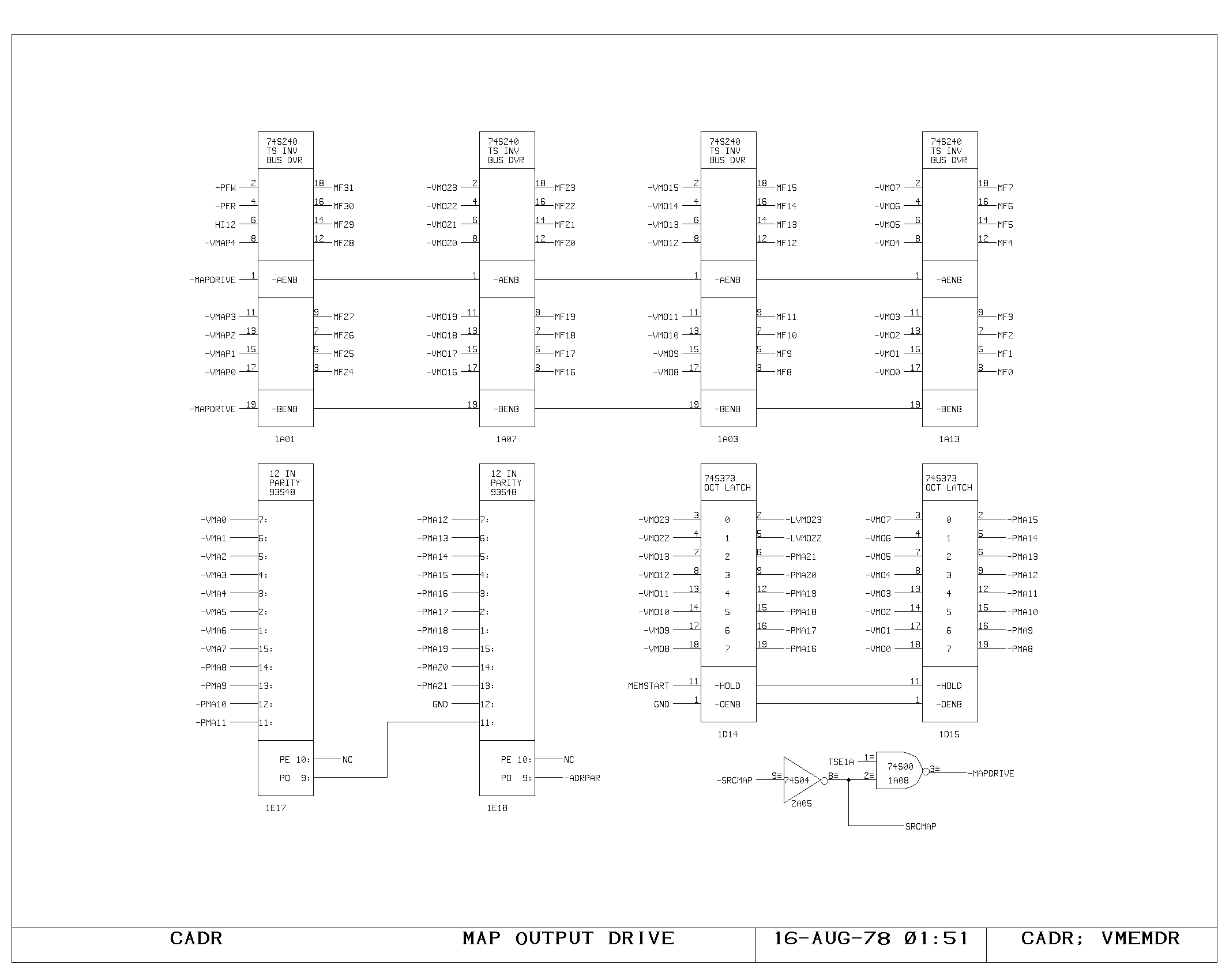
On a main memory read or write cycle, the map inputs are driven from
the VMA, and the map outputs, after settling, are held in the latches
shown on the VMEMDR print, such that the address sent to the memory
system is stable for the duration of the memory cycle. The final
memory address is formed from the low 8 bits of the VMA and the low 14
bits of the map outputs.
The VMEMDR print also contains drivers for the map outputs onto the MF
bus, so that the main data paths can access the map data. The
intermediate VMAP data is also driven onto the MF bus so that the
processor can distinguish first from second level map misses in the
paging microcode.
Writing of the map is done by addressing the map in the normal manner,
by loading a particular page entry into the MD register, and then
writing into the memories the data held in the VMA register.
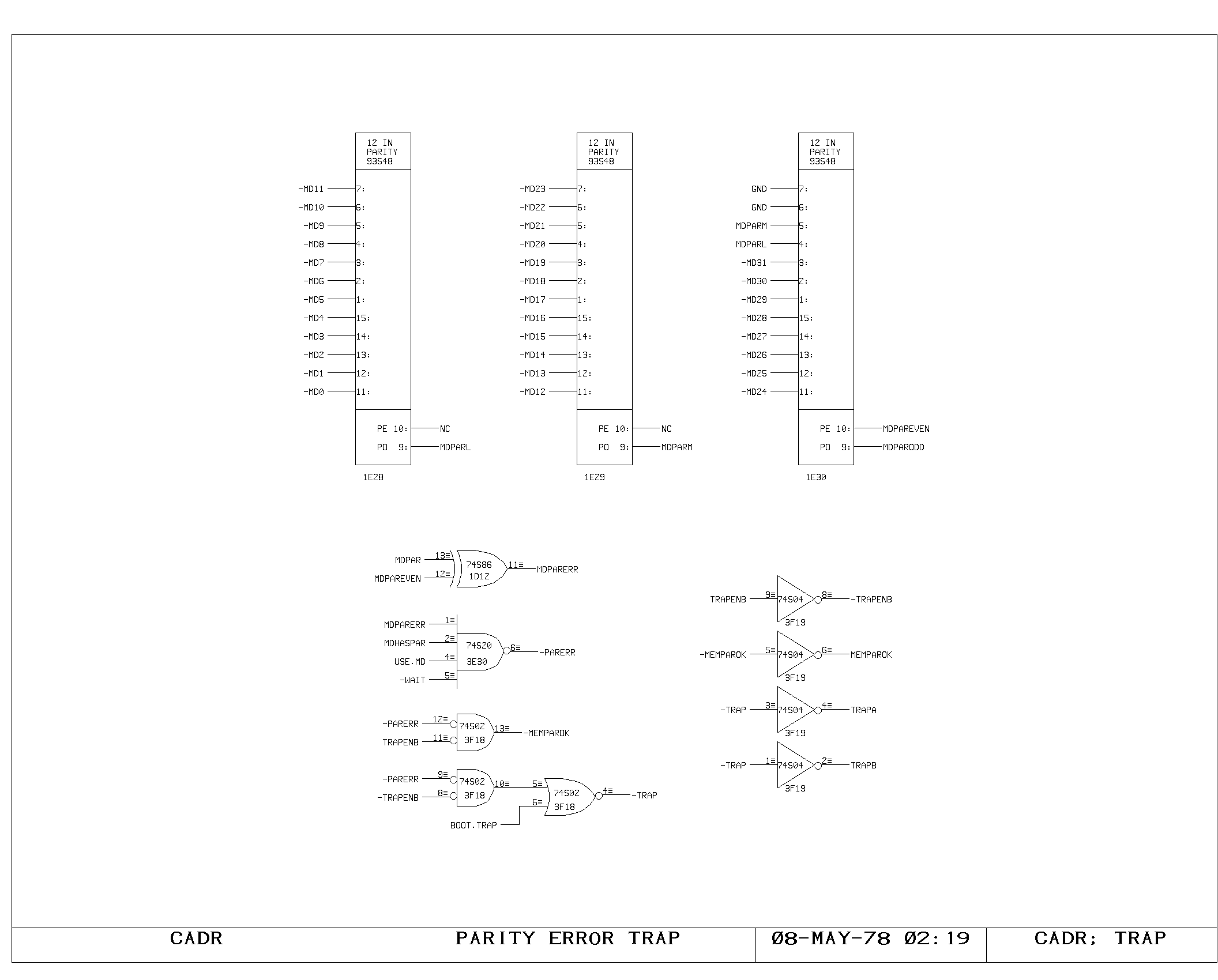
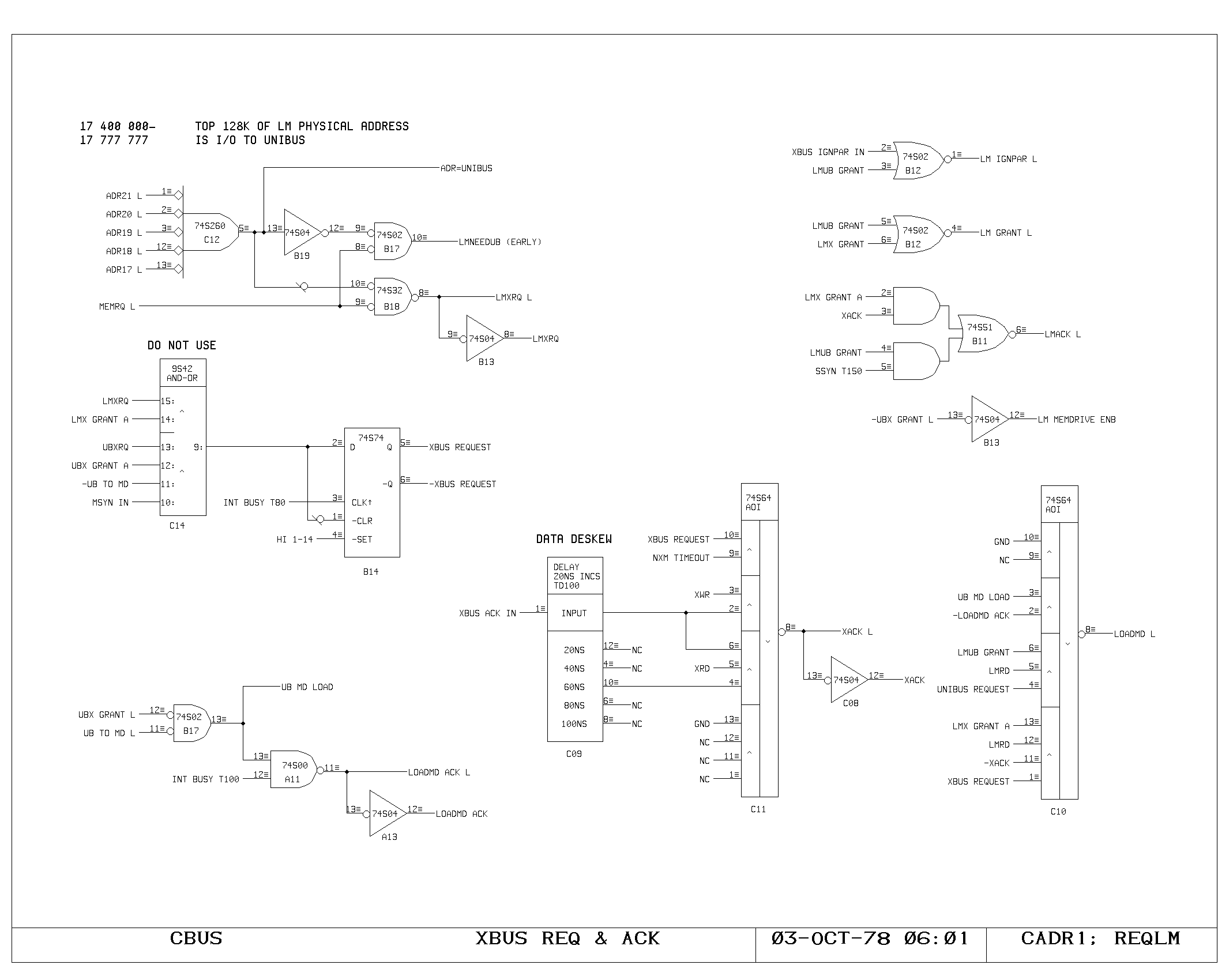
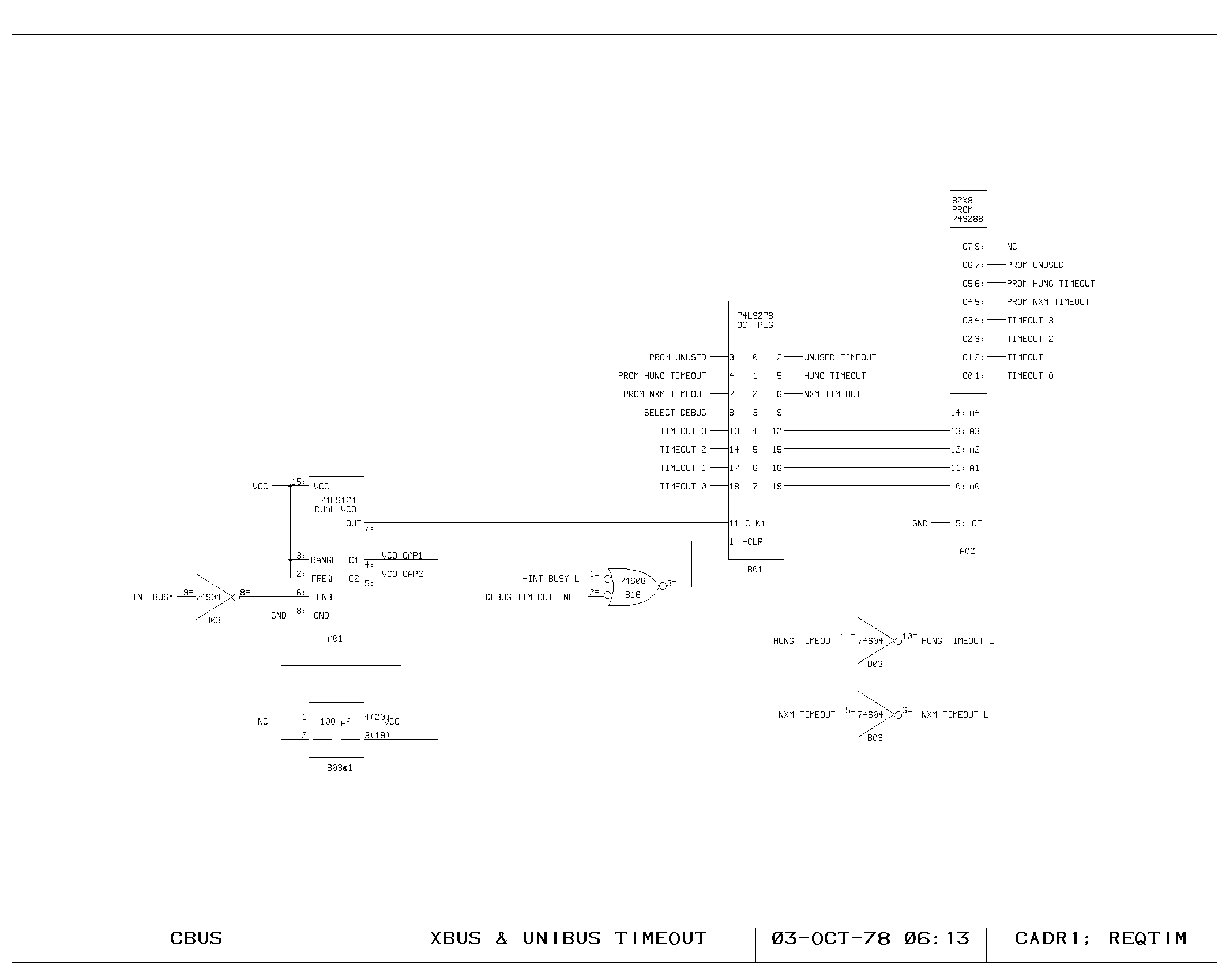
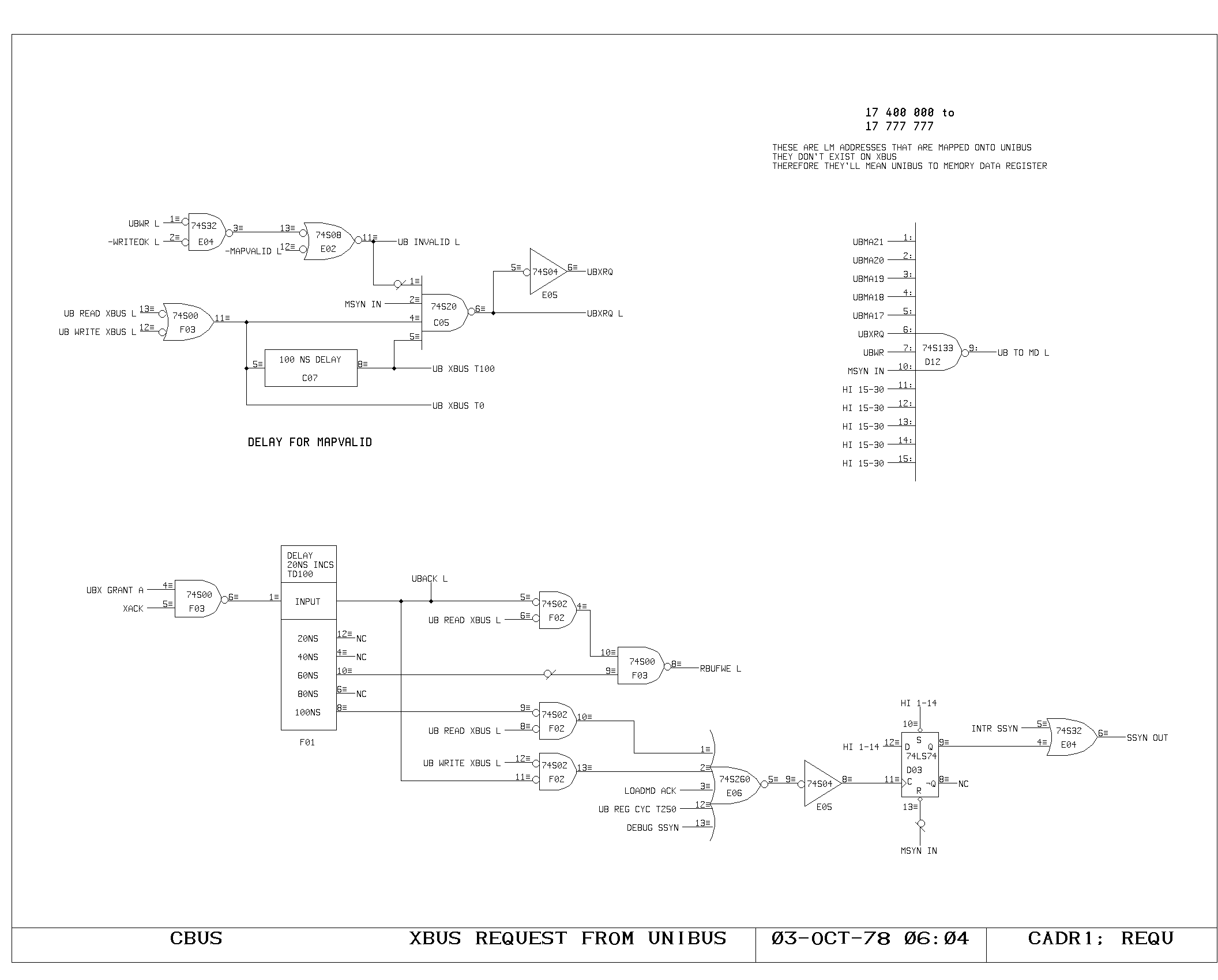
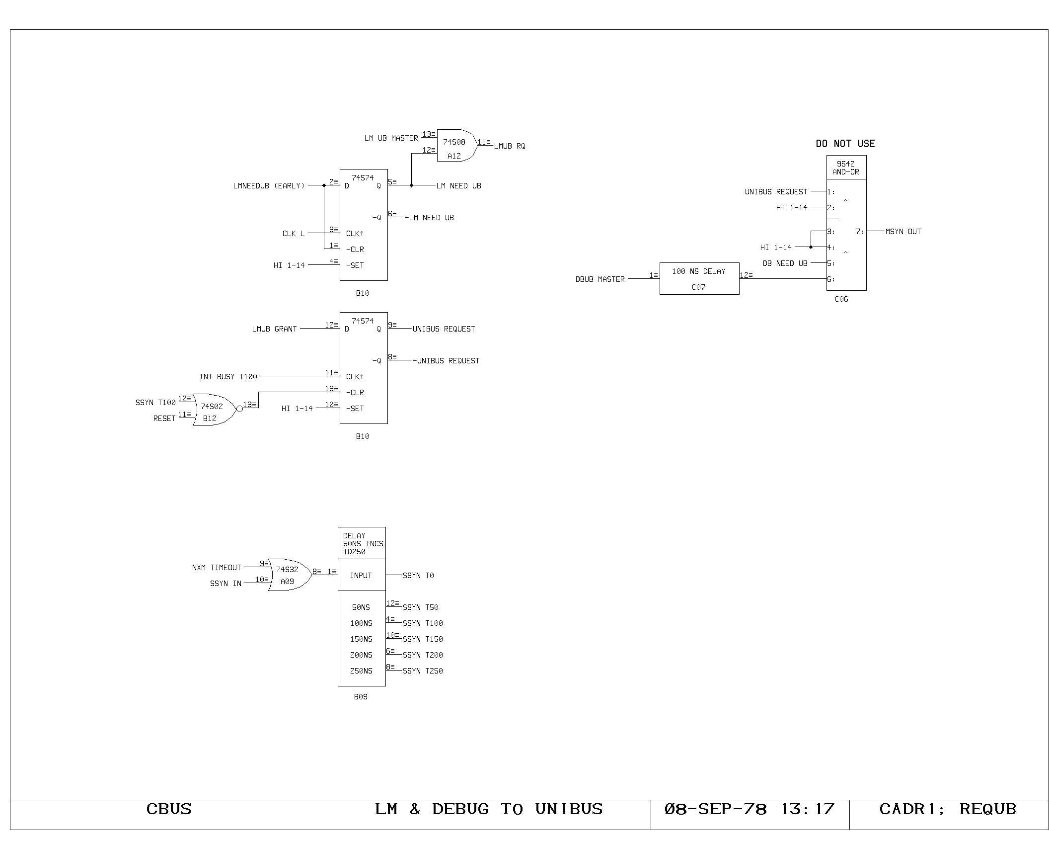
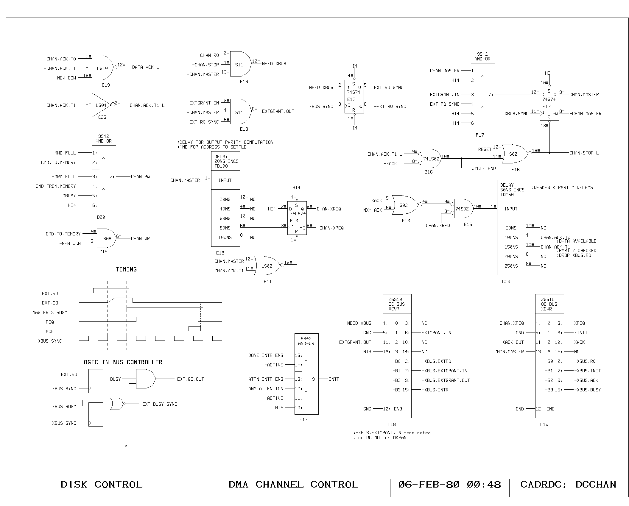
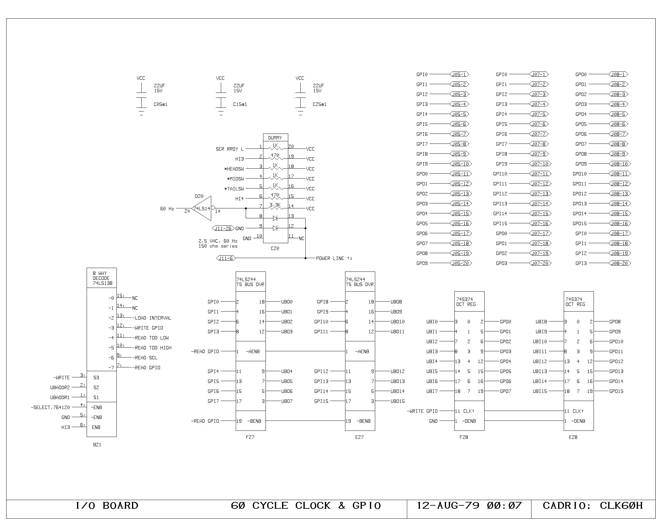
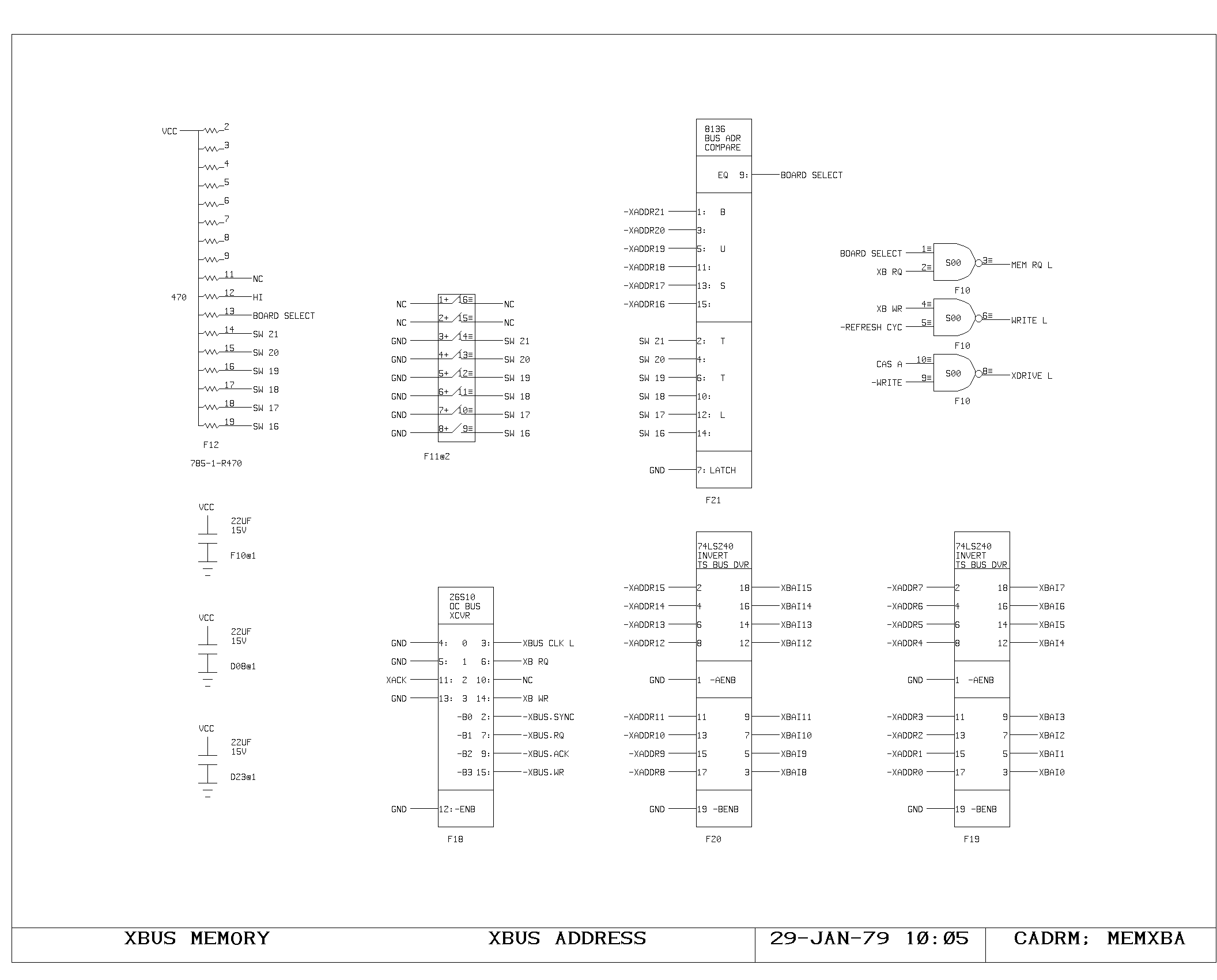
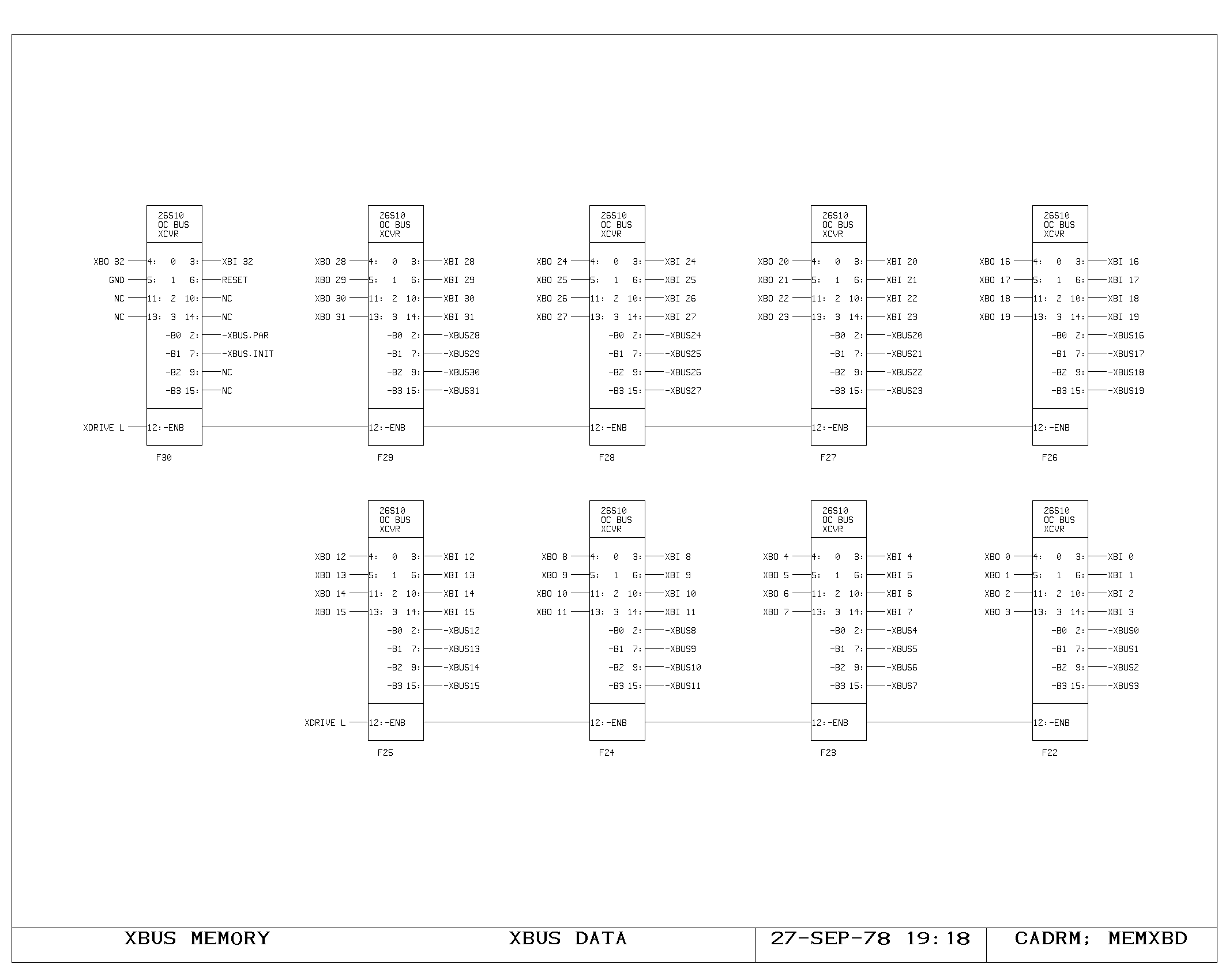
Memory Control Logic
The timing interface between the processor and the memory system is
handled on the VCTL1 and VCTL2 prints. These handle the timing of map
references, synchronization between the asynchronous bus and the
clocking of the processor, and detection of the cases when the
processor clock must be delayed pending arrival of data from the main
memory system.

Cycles are initiated with either a read, write, or instruction fetch
(-MEMRD, -MEMWR, -IFETCH) is required, and results in setting of the
MEMSTART flipflop. During the MEMSTART cycle, the map inputs are gated
from the VMA.

Assuming there was no map miss or protect violation, the request is
sent to the main memory system (MEMRQ) and memory busy is set
(MBUSY). On read cycles, RD.IN.PROGRESS is set. Execution of
microinstructions continues normally, unless one of the gates driving
HANG or WAIT causes the processor clock generator to momentarily halt,
after detecting the potential interference between the program
executing and the state of the memory system.